
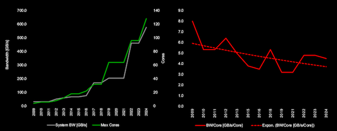
The compute market has always been hungry for memory bandwidth, particularly for high-performance applications in servers and datacenters. In recent years, the explosion in core counts per socket has further accentuated this need. Despite progress in DDR speeds, the available bandwidth per core has unfortunately not seen a corresponding scaling.
The stakeholders in the industry have been attempting to address this by building additional technology on top of existing widely-adopted memory standards. With DDR5, there are currently two technologies attempting to increase the peak bandwidth beyond the official speeds. In late 2022, SK hynix introduced MCR-DIMMs meant for operating with specific Intel server platforms. On the other hand, JEDEC - the standards-setting body - also developed specifications for MR-DIMMs with a similar approach. Both of them build upon existing DDR5 technologies by attempting to combine multiple ranks to improve peak bandwidth and latency.
The MR-DIMM standard is conceptually simple - there are multiple ranks of memory modules operating at standard DDR5 speeds with a data buffer in front. The buffer operates at 2x the speed on the host interface side, allowing for essentially double the transfer rates. The challenges obviously lie in being able to operate the logic in the host memory controller at the higher speed and keeping the power consumption / thermals in check.
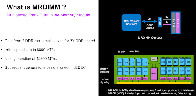
The first version of the JEDEC MR-DIMM standard specifies speeds of 8800 MT/s, with the next generation at 12800 MT/s. JEDEC also has a clear roadmap for this technology, keeping it in sync with the the improvements in the DDR5 standard.
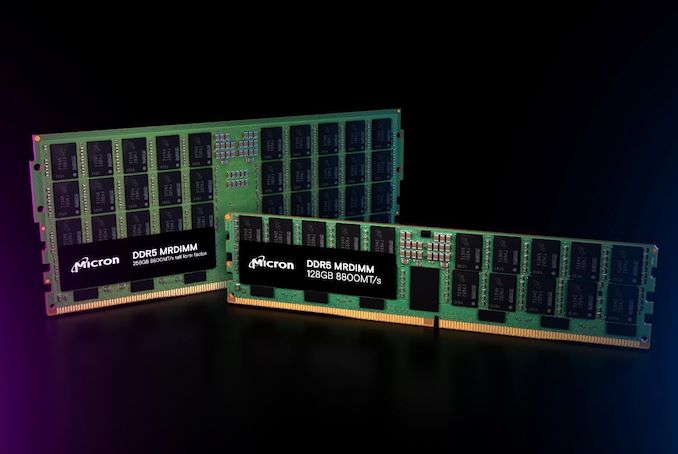
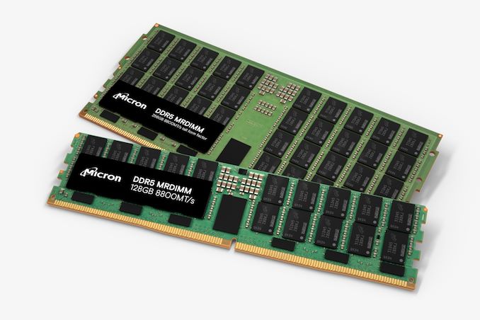
Micron and Intel have been working closely in the last few quarters to bring their former's first-generation MR-DIMM lineup to the market. Intel's Xeon 6 Family with P-Cores (Granite Rapids) is the first platform to bring MR-DIMM support at 8800 MT/s on the host side. Micron's standard-sized MR-DIMMs (suitable for 1U servers) and TFF (tall form-factor) MR-DIMMs (for 2U+ servers) have been qualified for use with the same.
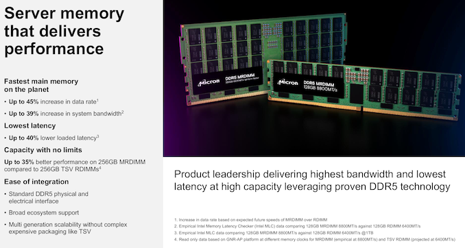
The benefits offered by MR-DIMMs are evident from the JEDEC specifications, allowing for increased data rates and system bandwidth, with improvements in latency. On the capacity side, allowing for additional ranks on the modules has enabled Micron to offer a 256 GB capacity point. It must be noted that some vendors are also using TSV (through-silicon vias) technology to to increase the per-package capacity at standard DDR5 speeds, but this adds additional cost and complexity that are largely absent in the MR-DIMM manufacturing process.
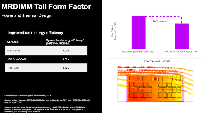
The tall form-factor (TFF) MR-DIMMs have a larger surface area compared to the standard-sized ones. For the same airflow configuration, this allows the DIMM to have a better thermal profile. This provides benefits for energy efficiency as well by reducing the possibility of thermal throttling.
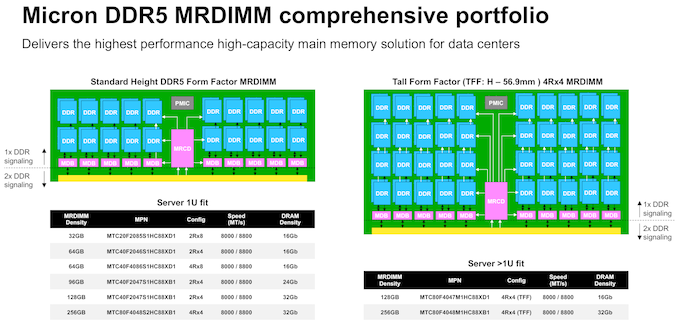
Micron is launching a comprehensive lineup of MR-DIMMs in both standard and tall form-factors today, with multiple DRAM densities and speed options as noted above.
Micron and Intel hosted a media / analyst briefing recently to demonstrate the benefits of MR-DIMMs for Xeon 6 with P-Cores (Granite Rapids). Using a 2P configuration with 96-core Xeon 6 processors, benchmarks for different ... Memory


Demand for high-performance processors for AI training is skyrocketing, and consequently so is the demand for the components that go into these processors. So much so that SK hynix this week is very publicly announcing that the company's high-bandwidth memory (HBM) production capacity has already sold out for the rest of 2024, and even most of 2025 has already sold out as well.
SK hynix currently produces various types of HBM memory for customers like Amazon, AMD, Facebook, Google (Broadcom), Intel, Microsoft, and, of course, NVIDIA. The latter is an especially prolific consumer of HBM3 and HBM3E memory for its H100/H200/GH200 accelerators, as NVIDIA is also working to fill what remains an insatiable (and unmet) demand for its accelerators.
As a result, HBM memory orders, which are already placed months in advance, are now backlogging well into 2025 as chip vendors look to secure supplies of the memory stacks critical to their success.
This has made SK hynix the secnd HBM memory vendor in recent months to announce that they've sold out into 2025, following an earlier announcement from Micron regarding its HBM3E production. But of the two announcements, SK hynix's is arguably the most significant yet, as the South Korean firm's HBM production capacity is far greater than Micron's. So while things were merely "interesting" with the smallest of the Big Three memory manufacturers being sold out into 2025, things are taking a more concerning (and constrained) outlook now that SK hynix is as well.
SK hynix currently controls roughly 46% - 49% of HBM market, and its share is not expected to drop significantly in 2025, according to market tracking firm TrendForce. By contrast, Micron's share on HBM memory market is between 4% and 6%. Since HBM supply of both companies is sold out through the most of 2025, we're likely looking at a scenario where over 50% of the industry's total HBM3/HBM3E supply for the coming quarters is already sold out.
This leaves Samsung as the only member of the group not to comment on HBM demand so far. Though with memory being a highly fungible commodity product, it would be surprising if Samsung wasn't facing similar demand. And, ultimately, all of this is pointing towards the indusry entering an HBM3 memory shortage.
Separately, SK hynix said that it is sampling 12-Hi 36GB HBM3E stacks with customers and will begin volume shipments in the third quarter.
Memory
As LPCAMM2 adoption begins, the first retail memory modules are finally starting to hit the retail market, courtesy of Micron. The memory manufacturer has begun selling their LPDDR5X-based LPCAMM2 memory modules under their in-house Crucial brand, making them available on the latter's storefront. Timed to coincide with the release of Lenovo's ThinkPad P1 Gen 7 laptop – the first retail laptop designed to use the memory modules – this marks the de facto start of the eagerly-awaited modular LPDDR5X memory era.
Micron's Low Power Compression Attached Memory Module 2 (LPCAMM2) modules are available in capacities of 32 GB and 64 GB. These are dual-channel modules that feature a 128-bit wide interface, and are based around LPDDR5X memory running at data rates up to 7500 MT/s. This gives a single LPCAMM2 a peak bandwidth of 120 GB/s. Micron is not disclosing the latencies of its LPCAMM2 memory modules, but it says that high data transfer rates of LPDDR5X compensate for the extended timings.
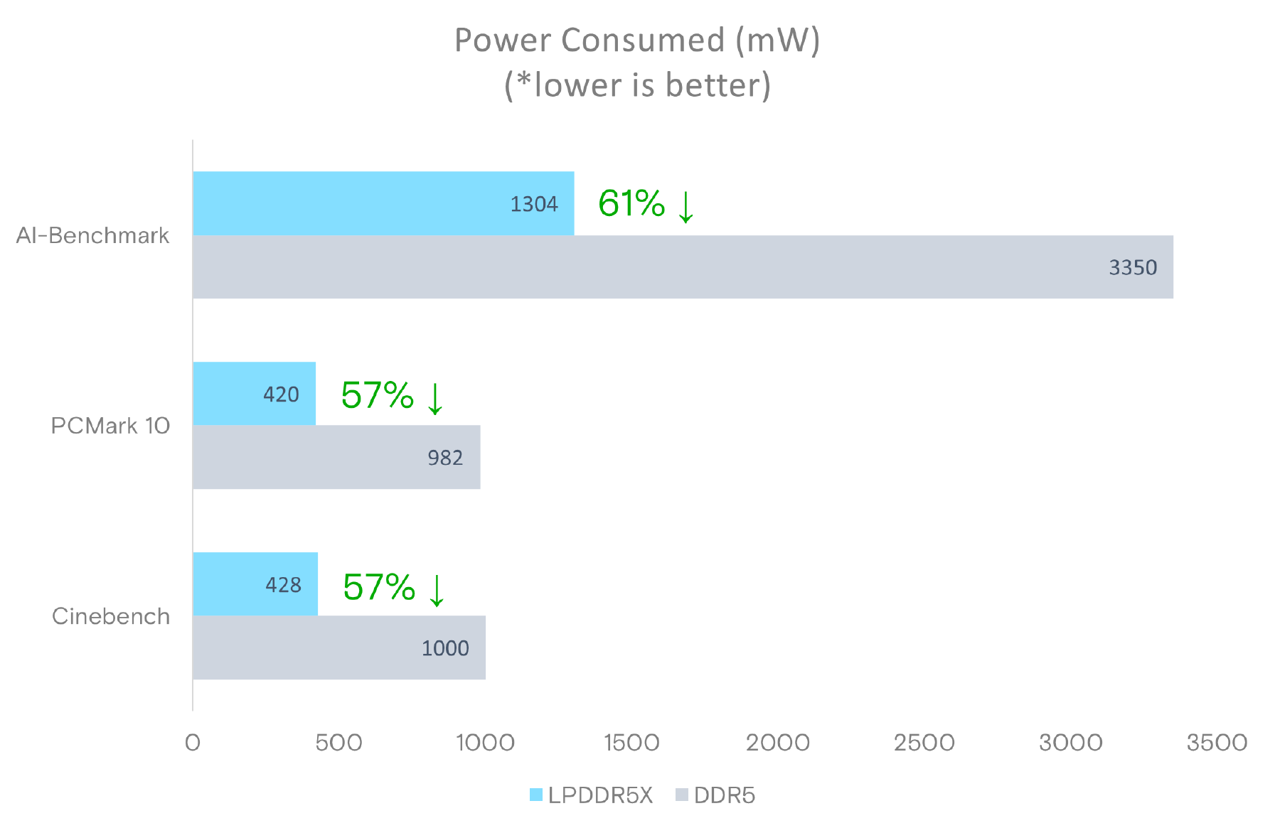
Micron says that LPDDR5X memory offers significantly lower power consumption, with active power per 64-bit bus being 43-58% lower than DDR5 at the same speed, and standby power up to 80% lower. Meanwhile, similar to DDR5 modules, LPCAMM2 modules include a power management IC and voltage regulating circuitry, which provides module manufacturers additional opportunities to reduce power consumption of their products.
Source: Micron LPDDR5X LPCAMM2 Technical Brief
It's worth noting, however, that at least for the first generation of LPCAMM2 modules, system vendors will need to pick between modularity and performance. While soldered-down LPDDR5X memory is available at speeds up to 8533 MT/sec – and with 9600 MT/sec on the horizon – the fastest LPCAMM2 modules planned for this year by both Micron and rival Samsung will be running at 7500 MT/sec. So vendors will have to choose between the flexibility of offering modular LPDDR5X, or the higher bandwidth (and space savings) offered by soldering down their memory.
Micron, for its part, is projecting that 9600 MT/sec LPCAMM2 modules will be available by 2026. Though it's all but certain that faster memory will also be avaialble in the same timeframe.
Micron's Crucial LPDDR5X 32 GB module costs $174.99, whereas a 64 GB module costs $329.99.
Memory
Demand for high-performance processors for AI training is skyrocketing, and consequently so is the demand for the components that go into these processors. So much so that SK hynix this week is very publicly announcing that the company's high-bandwidth memory (HBM) production capacity has already sold out for the rest of 2024, and even most of 2025 has already sold out as well.
SK hynix currently produces various types of HBM memory for customers like Amazon, AMD, Facebook, Google (Broadcom), Intel, Microsoft, and, of course, NVIDIA. The latter is an especially prolific consumer of HBM3 and HBM3E memory for its H100/H200/GH200 accelerators, as NVIDIA is also working to fill what remains an insatiable (and unmet) demand for its accelerators.
As a result, HBM memory orders, which are already placed months in advance, are now backlogging well into 2025 as chip vendors look to secure supplies of the memory stacks critical to their success.
This has made SK hynix the secnd HBM memory vendor in recent months to announce that they've sold out into 2025, following an earlier announcement from Micron regarding its HBM3E production. But of the two announcements, SK hynix's is arguably the most significant yet, as the South Korean firm's HBM production capacity is far greater than Micron's. So while things were merely "interesting" with the smallest of the Big Three memory manufacturers being sold out into 2025, things are taking a more concerning (and constrained) outlook now that SK hynix is as well.
SK hynix currently controls roughly 46% - 49% of HBM market, and its share is not expected to drop significantly in 2025, according to market tracking firm TrendForce. By contrast, Micron's share on HBM memory market is between 4% and 6%. Since HBM supply of both companies is sold out through the most of 2025, we're likely looking at a scenario where over 50% of the industry's total HBM3/HBM3E supply for the coming quarters is already sold out.
This leaves Samsung as the only member of the group not to comment on HBM demand so far. Though with memory being a highly fungible commodity product, it would be surprising if Samsung wasn't facing similar demand. And, ultimately, all of this is pointing towards the indusry entering an HBM3 memory shortage.
Separately, SK hynix said that it is sampling 12-Hi 36GB HBM3E stacks with customers and will begin volume shipments in the third quarter.
Memory
As LPCAMM2 adoption begins, the first retail memory modules are finally starting to hit the retail market, courtesy of Micron. The memory manufacturer has begun selling their LPDDR5X-based LPCAMM2 memory modules under their in-house Crucial brand, making them available on the latter's storefront. Timed to coincide with the release of Lenovo's ThinkPad P1 Gen 7 laptop – the first retail laptop designed to use the memory modules – this marks the de facto start of the eagerly-awaited modular LPDDR5X memory era.
Micron's Low Power Compression Attached Memory Module 2 (LPCAMM2) modules are available in capacities of 32 GB and 64 GB. These are dual-channel modules that feature a 128-bit wide interface, and are based around LPDDR5X memory running at data rates up to 7500 MT/s. This gives a single LPCAMM2 a peak bandwidth of 120 GB/s. Micron is not disclosing the latencies of its LPCAMM2 memory modules, but it says that high data transfer rates of LPDDR5X compensate for the extended timings.
Micron says that LPDDR5X memory offers significantly lower power consumption, with active power per 64-bit bus being 43-58% lower than DDR5 at the same speed, and standby power up to 80% lower. Meanwhile, similar to DDR5 modules, LPCAMM2 modules include a power management IC and voltage regulating circuitry, which provides module manufacturers additional opportunities to reduce power consumption of their products.
Source: Micron LPDDR5X LPCAMM2 Technical Brief
It's worth noting, however, that at least for the first generation of LPCAMM2 modules, system vendors will need to pick between modularity and performance. While soldered-down LPDDR5X memory is available at speeds up to 8533 MT/sec – and with 9600 MT/sec on the horizon – the fastest LPCAMM2 modules planned for this year by both Micron and rival Samsung will be running at 7500 MT/sec. So vendors will have to choose between the flexibility of offering modular LPDDR5X, or the higher bandwidth (and space savings) offered by soldering down their memory.
Micron, for its part, is projecting that 9600 MT/sec LPCAMM2 modules will be available by 2026. Though it's all but certain that faster memory will also be avaialble in the same timeframe.
Micron's Crucial LPDDR5X 32 GB module costs $174.99, whereas a 64 GB module costs $329.99.
Memory
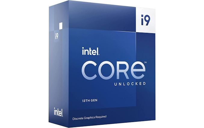
In an unexpected move, Intel has announced plans to phase out the boxed versions of its enthusiasts-class 13th Generation Core 'Raptor Lake' processors. According to a product change notification (PCN) published by the company last month, Intel plans to stop shipping these desktop CPUs by late June. In its place will remain Intel's existing lineup of boxed 14th Generation Core processors, which are based on the same 'Raptor Lake' silicon and typically carry higher performance for similar prices.
Intel customers and distributors interested in getting boxed versions 13th Generation Core i5-13600K/KF, Core i7-13700K/KF, and Core i9-13900K/KF/KS 'Raptor Lake' processors with unlocked multiplier should place their orders by May 24, 2024. The company will ship these units by June 28, 2024. Meanwhile, the PCN does not mention any change to the availability of tray versions of these CPUs, which are sold to OEMs and wholesalers.
The impending discontinuation of Intel's boxed 13th Generation Core processors comes as the company's current 14th Generation product line, 'Raptor Lake Refresh' is largely a rehash of the same silicon at slightly higher clockspeeds. Case in point: all of the discontinued SKUs are based on Intel's B0 Raptor Lake silicon, which is still being used for their 14th Gen counterparts. So Intel has not discontinued producing any Raptor Lake silicon; only the number of retail SKUs is getting cut-down.
As outlined in our 14th Generation Core/Raptor Lake Refresh review, the 14th Gen chips largely make their 13th Gen counterparts redundant, offering better performance at every tier for the same list price. And with virtually all current generation motherboards supporting both generation of chips, apparently Intel feels there's little reason to keep around what's essentially older, slower SKUs of the same silicon.
Interestingly, the retirement of the enthusiast-class 13th Generation Core chips is coming before Intel discontinues their even older 12th Generation Core 'Alder Lake' processors. 12th Gen chips are still available to this day in both boxed and tray versions, and the Alder Lake silicon itself is still widely in use in multiple product families. So even though Alder Lake shares the same platform as Raptor Lake, the chips based on that silicon haven't been rendered redundant in the same way that 13th Gen Core chips have.
Ultimately, it would seem that Intel is intent on consolidating and simplifying its boxed retail chip offerings by retiring their near-duplicate SKUs. Which for PC buyers could present a minor opportunity for a deal, as retailers work to sell off their remaining 13th Gen enthusiast chips.
CPUs
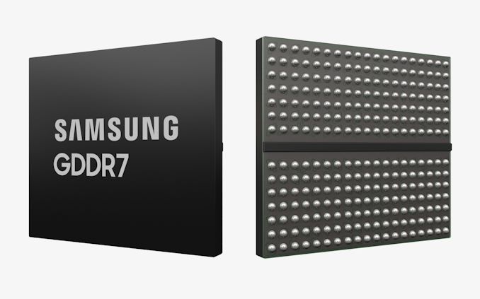
Now that JEDEC has published specification of GDDR7 memory, memory manufacturers are beginning to announce their initial products. The first out of the gate for this generation is Samsung, which has has quietly added its GDDR7 products to its official product catalog.
For now, Samsung lists two GDDR7 devices on its website: 16 Gbit chips rated for an up to 28 GT/s data transfer rate and a faster version running at up to 32 GT/s data transfer rate (which is in line with initial parts that Samsung announced in mid-2023). The chips feature a 512M x32 organization and come in a 266-pin FBGA packaging. The chips are already sampling, so Samsung's customers – GPU vendors, AI inference vendors, network product vendors, and the like – should already have GDDR7 chips in their labs.
The GDDR7 specification promises the maximum per-chip capacity of 64 Gbit (8 GB) and data transfer rates of 48 GT/s. Meanwhile, first generation GDDR7 chips (as announced so far) will feature a rather moderate capacity of 16 Gbit (2 GB) and a data transfer rate of up to 32 GT/s.
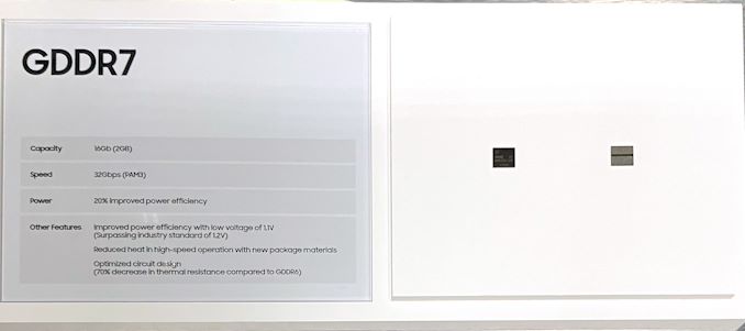
Performance-wise, the first generation of GDDR7 should provide a significant improvement in memory bandwidth over GDDR6 and GDDR6X. However capacity/density improvements will not come until memory manufacturers move to their next generation EUV-based process nodes. As a result, the first GDDR7-based graphics cards are unlikely to sport any memory capacity improvements. Though looking a bit farther down the road, Samsung and SK Hynix have previously told Tom's Hardware that they intend to reach mass production of 24 Gbit GDDR7 chips in 2025.
Otherwise, it is noteworthy that SK Hynix also demonstrated its GDDR7 chips at NVIDIA's GTC last week. So Samsung's competition should be close behind in delivering samples, and eventually mass production memory.
Source: Samsung (via @harukaze5719)
Memory
In an unexpected move, Intel has announced plans to phase out the boxed versions of its enthusiasts-class 13th Generation Core 'Raptor Lake' processors. According to a product change notification (PCN) published by the company last month, Intel plans to stop shipping these desktop CPUs by late June. In its place will remain Intel's existing lineup of boxed 14th Generation Core processors, which are based on the same 'Raptor Lake' silicon and typically carry higher performance for similar prices.
Intel customers and distributors interested in getting boxed versions 13th Generation Core i5-13600K/KF, Core i7-13700K/KF, and Core i9-13900K/KF/KS 'Raptor Lake' processors with unlocked multiplier should place their orders by May 24, 2024. The company will ship these units by June 28, 2024. Meanwhile, the PCN does not mention any change to the availability of tray versions of these CPUs, which are sold to OEMs and wholesalers.
The impending discontinuation of Intel's boxed 13th Generation Core processors comes as the company's current 14th Generation product line, 'Raptor Lake Refresh' is largely a rehash of the same silicon at slightly higher clockspeeds. Case in point: all of the discontinued SKUs are based on Intel's B0 Raptor Lake silicon, which is still being used for their 14th Gen counterparts. So Intel has not discontinued producing any Raptor Lake silicon; only the number of retail SKUs is getting cut-down.
As outlined in our 14th Generation Core/Raptor Lake Refresh review, the 14th Gen chips largely make their 13th Gen counterparts redundant, offering better performance at every tier for the same list price. And with virtually all current generation motherboards supporting both generation of chips, apparently Intel feels there's little reason to keep around what's essentially older, slower SKUs of the same silicon.
Interestingly, the retirement of the enthusiast-class 13th Generation Core chips is coming before Intel discontinues their even older 12th Generation Core 'Alder Lake' processors. 12th Gen chips are still available to this day in both boxed and tray versions, and the Alder Lake silicon itself is still widely in use in multiple product families. So even though Alder Lake shares the same platform as Raptor Lake, the chips based on that silicon haven't been rendered redundant in the same way that 13th Gen Core chips have.
Ultimately, it would seem that Intel is intent on consolidating and simplifying its boxed retail chip offerings by retiring their near-duplicate SKUs. Which for PC buyers could present a minor opportunity for a deal, as retailers work to sell off their remaining 13th Gen enthusiast chips.
CPUs
Following a relative lull in the desktop memory industry in the previous decade, the past few years have seen a flurry of new memory standards and form factors enter development. Joining the traditional DIMM/SO-DIMM form factors, we've seen the introduction of space-efficient DDR5 CAMM2s, their LPDDR5-based counterpart the LPCAMM2, and the high-clockspeed optimized CUDIMM. But JEDEC, the industry organization behind these efforts, is not done there. In a press release sent out at the start of the week, the group announced that it is working on standards for DDR5 Multiplexed Rank DIMMs (MRDIMM) for servers, as well as an updated LPCAMM standard to go with next-generation LPDDR6 memory.
Just last week Micron introduced the industry's first DDR5 MRDIMMs, which are timed to launch alongside Intel's Xeon 6 server platforms. But while Intel and its partners are moving full steam ahead on MRDIMMs, the MRDIMM specification has not been fully ratified by JEDEC itself. All told, it's not unusual to see Intel pushing the envelope here on new memory technologies (the company is big enough to bootstrap its own ecosystem). But as MRDIMMs are ultimately meant to be more than just a tool for Intel, a proper industry standard is still needed – even if that takes a bit longer.
Under the hood, MRDIMMs continue to use DDR5 components, form-factor, pinout, SPD, power management ICs (PMICs), and thermal sensors. The major change with the technology is the introduction of multiplexing, which combines multiple data signals over a single channel. The MRDIMM standard also adds RCD/DB logic in a bid to boost performance, increase capacity of memory modules up to 256 GB (for now), shrink latencies, and reduce power consumption of high-end memory subsystems. And, perhaps key to MRDIMM adoption, the standard is being implemented as a backwards-compatible extension to traditional DDR5 RDIMMs, meaning that MRDIMM-capable servers can use either RDIMMs or MRDIMMs, depending on how the operator opts to configure the system.
The MRDIMM standard aims to double the peak bandwidth to 12.8 Gbps, increasing pin speed and supporting more than two ranks. Additionally, a "Tall MRDIMM" form factor is in the works (and pictured above), which is designed to allow for higher capacity DIMMs by providing more area for laying down memory chips. Currently, ultra high capacity DIMMs require using expensive, multi-layer DRAM packages that use through-silicon vias (3DS packaging) to attach the individual DRAM dies; a Tall MRDIMM, on the other hand, can just use a larger number of commodity DRAM chips. Overall, the Tall MRDIMM form factor enables twice the number of DRAM single-die packages on the DIMM.
Meanwhile, this week's announcement from JEDEC offers the first significant insight into what to expect from LPDDR6 CAMMs. And despite LPDDR5 CAMMs having barely made it out the door, some significant shifts with LPDDR6 itself means that JEDEC will need to make some major changes to the CAMM standard to accommodate the newer memory type.
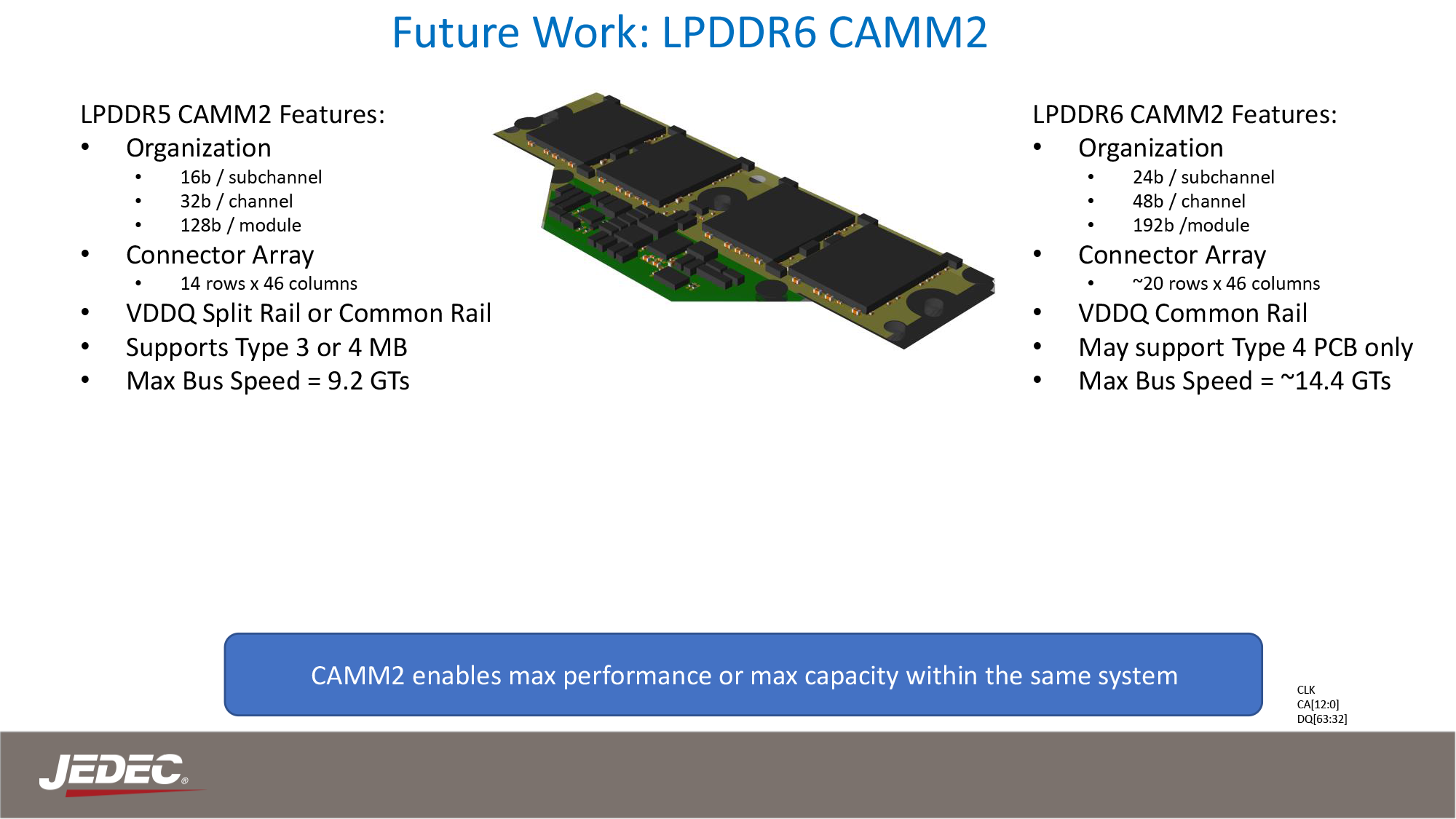
JEDEC Presentation: The CAMM2 Journey and Future Potential
Besides the higher memory clockspeeds allowed by LPDDR6 – JEDEC is targeting data transfer rates of 14.4 GT/s and higher – the new memory form-factor will also incorporate an altogether new connector array. This is to accommodate LPDDR6's wider memory bus, which sees the channel width of an individual memory chip grow from 16-bits wide to 24-bits wide. As a result, the current LPCAMM design, which is intended to match the PC standard of a cumulative 128-bit (16x8) design needs to be reconfigured to match LPDDR6's alterations.
Ultimately, JEDEC is targeting a 24-bit subhannel/48-bit channel design, which will result in a 192-bit wide LPCAMM. While the LPCAMM connector itself is set to grow from 14 rows of pins to possibly as high as 20. New memory technologies typically require new DIMMs to begin with, so it's important to clarify that this is not unexpected, but at th... Memory

![]()
In addition to revealing its roadmap and plans concerning its current leading-edge process technologies, TSMC also shared progress of its N2 node as part of its Symposiums 2024. The company's first 2nm-class fabrication node, and predominantly featuring gate-all-around transistors, according to TSMC N2 has almost achieved its target performance and yield goals, which places it on track to enter high-volume manufacturing in the second half of 2025.
TSMC states that 'N2 development is well on track and N2P is next.' In particular, gate-all-around nanosheet devices currently achieve over 90% of their expected performance, whereas yields of 256 Mb SRAM (32 MB) devices already exceeds 80%, depending on the batch. All of this for a node that is over a year away from mass production.
Meanwhile, average yield of a 256 Mb SRAM was around 70% as of March, 2024, up from around 35% in April, 2023. Device performance has also been improving with higher frequencies being achieved while keeping power consumption in check.
Chip designer interest towards TSMC's first 2nm-class gate-all-around nanosheet transistor-based technology is significant, too. The number of new tape-outs (NTOs) in the first year of N2 is over two-times higher than it was for N5. Though with that said, given TSMC's close working relationship with a handful of high-volume vendors – most notably Appe – NTOs can be a very misleading figure since the first year of a new node at TSMC is capacity constrained, and consequently the bulk of that capacity goes to TSMC's priority partners.
Meanwhile, there were considerably more N5 tapeouts in its second year (some where N5P, of course) and N2 promises to have 2.6X more NTOs in its second year. So the node indeed looks quite promising. In fact, based on TSMC's slides (which we're unfortunately not able to republish), N2 is more popular than N3 in terms of NTOs both in the first and the second years of existence.
When it comes to the second year of N2, in the second half of 2026 TSMC plans to roll out its N2P technology, which promises additional performance and power benefits. N2P is expected to improve frequency by 15% - 20%, reduce power consumption by 30% - 40%, and increase chip density by over 1.15 times compared to N3E, significant benefits to move to all-new GAA nanosheet transistors.
Finally, for those companies that need the best in performance, power, and density, TSMC is poised to offer their A16 process in 2026. That node will also bring in backside power delivery, which will add costs, but is expected to greatly improve performance efficiency and scaling.
Semiconductors
Lorem Ipsum is simply dummy text of the printing and typesetting industry. Lorem Ipsum has been the industry's.
Demand for high-performance processors for AI training is skyrocketing, and consequently so is the demand for the components that go into these processors. So much so that SK hynix this week is very publicly announcing that the company's high-bandwidth memory (HBM) production capacity has already sold out for the rest of 2024, and even most of 2025 has already sold out as well.
SK hynix currently produces various types of HBM memory for customers like Amazon, AMD, Facebook, Google (Broadcom), Intel, Microsoft, and, of course, NVIDIA. The latter is an especially prolific consumer of HBM3 and HBM3E memory for its H100/H200/GH200 accelerators, as NVIDIA is also working to fill what remains an insatiable (and unmet) demand for its accelerators.
As a result, HBM memory orders, which are already placed months in advance, are now backlogging well into 2025 as chip vendors look to secure supplies of the memory stacks critical to their success.
This has made SK hynix the secnd HBM memory vendor in recent months to announce that they've sold out into 2025, following an earlier announcement from Micron regarding its HBM3E production. But of the two announcements, SK hynix's is arguably the most significant yet, as the South Korean firm's HBM production capacity is far greater than Micron's. So while things were merely "interesting" with the smallest of the Big Three memory manufacturers being sold out into 2025, things are taking a more concerning (and constrained) outlook now that SK hynix is as well.
SK hynix currently controls roughly 46% - 49% of HBM market, and its share is not expected to drop significantly in 2025, according to market tracking firm TrendForce. By contrast, Micron's share on HBM memory market is between 4% and 6%. Since HBM supply of both companies is sold out through the most of 2025, we're likely looking at a scenario where over 50% of the industry's total HBM3/HBM3E supply for the coming quarters is already sold out.
This leaves Samsung as the only member of the group not to comment on HBM demand so far. Though with memory being a highly fungible commodity product, it would be surprising if Samsung wasn't facing similar demand. And, ultimately, all of this is pointing towards the indusry entering an HBM3 memory shortage.
Separately, SK hynix said that it is sampling 12-Hi 36GB HBM3E stacks with customers and will begin volume shipments in the third quarter.
Memory
As LPCAMM2 adoption begins, the first retail memory modules are finally starting to hit the retail market, courtesy of Micron. The memory manufacturer has begun selling their LPDDR5X-based LPCAMM2 memory modules under their in-house Crucial brand, making them available on the latter's storefront. Timed to coincide with the release of Lenovo's ThinkPad P1 Gen 7 laptop – the first retail laptop designed to use the memory modules – this marks the de facto start of the eagerly-awaited modular LPDDR5X memory era.
Micron's Low Power Compression Attached Memory Module 2 (LPCAMM2) modules are available in capacities of 32 GB and 64 GB. These are dual-channel modules that feature a 128-bit wide interface, and are based around LPDDR5X memory running at data rates up to 7500 MT/s. This gives a single LPCAMM2 a peak bandwidth of 120 GB/s. Micron is not disclosing the latencies of its LPCAMM2 memory modules, but it says that high data transfer rates of LPDDR5X compensate for the extended timings.
Micron says that LPDDR5X memory offers significantly lower power consumption, with active power per 64-bit bus being 43-58% lower than DDR5 at the same speed, and standby power up to 80% lower. Meanwhile, similar to DDR5 modules, LPCAMM2 modules include a power management IC and voltage regulating circuitry, which provides module manufacturers additional opportunities to reduce power consumption of their products.
Source: Micron LPDDR5X LPCAMM2 Technical Brief
It's worth noting, however, that at least for the first generation of LPCAMM2 modules, system vendors will need to pick between modularity and performance. While soldered-down LPDDR5X memory is available at speeds up to 8533 MT/sec – and with 9600 MT/sec on the horizon – the fastest LPCAMM2 modules planned for this year by both Micron and rival Samsung will be running at 7500 MT/sec. So vendors will have to choose between the flexibility of offering modular LPDDR5X, or the higher bandwidth (and space savings) offered by soldering down their memory.
Micron, for its part, is projecting that 9600 MT/sec LPCAMM2 modules will be available by 2026. Though it's all but certain that faster memory will also be avaialble in the same timeframe.
Micron's Crucial LPDDR5X 32 GB module costs $174.99, whereas a 64 GB module costs $329.99.
Memory


![TSMC to Expand Specialty Capacity by 50%, Introduce 4nm N4e Low-Power Node <p align="center"><a href="https://www.anandtech.com/show/21397/tsmc-to-expand-specialty-capacity-by-50-introduce-4nm-lowpower-node"><img src="https://images.anandtech.com/doci/21397/tsmc-semiconductor-fab-wafer-1-678_575px.jpg" alt="" /></a></p><p><p>With all the new fabs being built in Germany and Japan, as well as the expansion of production capacity in China, TSMC is planning to extend its production capacity for specialty technologies by 50% by 2027. As disclosed by the company during its European Technology Symposium this week, TSMC expects to need to not only convert existing capacity to meet demands for specialty processes, but even build new (greenfield) fab space just for this purpose. One of the big drivers for this demand, in turn, will be TSMC's next specialty node: N4e, a 4nm-class ultra-low-power production node.</p>
<p>"In the past, we always did the review phase [for upcoming fabs], but for the first time in a long time at TSMC, we started building greenfield fab that will address the future specialty technology requirements," said Dr. Kevin Zhang, Senior Vice President, Business Development and Overseas Operations Office, at the event. "In the next four to five years, we actually going to grow our specialty capacity by up to 1.5x. In doing so we actually expanding the footprint of our manufacturing network to improve the resiliency of the overall fab supply chain."</p>
<p>On top of its well-known major logic nodes like N5 and N3E, TSMC also offers a suite of specialty nodes for applications such as power semiconductors, mixed analog I/O, and ultra-low-power applications (e.g. IoT). These are typically based on the company's trailing manufacturing processes, but regardless of the underlying technology, the capacity demand for these nodes is growing right alongside the demand for TSMC's major logic nodes. All of which has required TSMC to reevaluate how they go about planning for capacity on their specialty nodes.</p>
<p>TSMC's expansion strategy in the recent years has pursued several goals. One of them has been to build new fabs outside of Taiwan; another has been to generally expand production capacity to meet future demand for all types of process technologies – which is why the company is building up capacity for specialty nodes.</p>
<p>At present, TSMC's most advanced specialty node is N6e, an N7/N6 variant that supports operating voltages between 0.4V and 0.9V. With N4e, TSMC is looking at voltages below 0.4V. Though for now, TSMC is not disclosing much in the way of technical details for the planned node; given the company's history here, we expect they'll have more to talk about next year once the new process is ready.</p>
</p> Semiconductors](https://lh3.googleusercontent.com/blogger_img_proxy/AEn0k_tesj1VdGmKPHAs6U14MrQnq79RyzokDMvIdnKUn2ZVbScavhkPO-lWYlc806JUkNK0FAhKRryWnNF5xsfOjI2U4sN1MCBpWBtoFHfsrQ0-YUlexxGxO7n1jj3UZNN5cMJTGqJfFyrROAXtIO25RvMsrZ37d_N7yQ=w72-h72-p-k-no-nu)
 is the first platform to bring MR-DIMM support at 8800 MT/s on the host side. Micron's standard-sized MR-DIMMs (suitable for 1U servers) and TFF (tall form-factor) MR-DIMMs (for 2U+ servers) have been qualified for use with the same.</p>
<p align="center"><a href="https://www.anandtech.com/show/21470/micron-mrdimm-lineup-expands-datacenter-dram-portfolio"><img alt="" src="https://images.anandtech.com/doci/21470/micron-mrdimm-lineup-intro_575px.png" /></a></p>
<p>The benefits offered by MR-DIMMs are evident from the JEDEC specifications, allowing for increased data rates and system bandwidth, with improvements in latency. On the capacity side, allowing for additional ranks on the modules has enabled Micron to offer a 256 GB capacity point. It must be noted that some vendors are also using TSV (through-silicon vias) technology to to increase the per-package capacity at standard DDR5 speeds, but this adds additional cost and complexity that are largely absent in the MR-DIMM manufacturing process.</p>
<p align="center"><a href="https://www.anandtech.com/show/21470/micron-mrdimm-lineup-expands-datacenter-dram-portfolio"><img alt="" src="https://images.anandtech.com/doci/21470/micron-mrdimm-tff-benefits_575px.png" /></a></p>
<p>The tall form-factor (TFF) MR-DIMMs have a larger surface area compared to the standard-sized ones. For the same airflow configuration, this allows the DIMM to have a better thermal profile. This provides benefits for energy efficiency as well by reducing the possibility of thermal throttling.</p>
<p align="center"><a href="https://www.anandtech.com/show/21470/micron-mrdimm-lineup-expands-datacenter-dram-portfolio"><img alt="" src="https://images.anandtech.com/doci/21470/micron-mrdimm-lineup-skus_575px.png" /></a></p>
<p>Micron is launching a comprehensive lineup of MR-DIMMs in both standard and tall form-factors today, with multiple DRAM densities and speed options as noted above.</p>
<h3>MRDIMM Benefits - Intel Granite Rapids Gets a Performance Boost</h3>
<p>Micron and Intel hosted a media / analyst briefing recently to demonstrate the benefits of MR-DIMMs for Xeon 6 with P-Cores (Granite Rapids). Using a 2P configuration with 96-core Xeon 6 processors, benchmarks for different ... Memory)
 is the first platform to bring MR-DIMM support at 8800 MT/s on the host side. Micron's standard-sized MR-DIMMs (suitable for 1U servers) and TFF (tall form-factor) MR-DIMMs (for 2U+ servers) have been qualified for use with the same.</p>
<p align="center"><a href="https://www.anandtech.com/show/21470/micron-mrdimm-lineup-expands-datacenter-dram-portfolio"><img alt="" src="https://images.anandtech.com/doci/21470/micron-mrdimm-lineup-intro_575px.png" /></a></p>
<p>The benefits offered by MR-DIMMs are evident from the JEDEC specifications, allowing for increased data rates and system bandwidth, with improvements in latency. On the capacity side, allowing for additional ranks on the modules has enabled Micron to offer a 256 GB capacity point. It must be noted that some vendors are also using TSV (through-silicon vias) technology to to increase the per-package capacity at standard DDR5 speeds, but this adds additional cost and complexity that are largely absent in the MR-DIMM manufacturing process.</p>
<p align="center"><a href="https://www.anandtech.com/show/21470/micron-mrdimm-lineup-expands-datacenter-dram-portfolio"><img alt="" src="https://images.anandtech.com/doci/21470/micron-mrdimm-tff-benefits_575px.png" /></a></p>
<p>The tall form-factor (TFF) MR-DIMMs have a larger surface area compared to the standard-sized ones. For the same airflow configuration, this allows the DIMM to have a better thermal profile. This provides benefits for energy efficiency as well by reducing the possibility of thermal throttling.</p>
<p align="center"><a href="https://www.anandtech.com/show/21470/micron-mrdimm-lineup-expands-datacenter-dram-portfolio"><img alt="" src="https://images.anandtech.com/doci/21470/micron-mrdimm-lineup-skus_575px.png" /></a></p>
<p>Micron is launching a comprehensive lineup of MR-DIMMs in both standard and tall form-factors today, with multiple DRAM densities and speed options as noted above.</p>
<h3>MRDIMM Benefits - Intel Granite Rapids Gets a Performance Boost</h3>
<p>Micron and Intel hosted a media / analyst briefing recently to demonstrate the benefits of MR-DIMMs for Xeon 6 with P-Cores (Granite Rapids). Using a 2P configuration with 96-core Xeon 6 processors, benchmarks for different ... Memory | https://compbuddey.blogspot.com/2024/07/micron-expands-datacenter-dram_18.html)
 is the first platform to bring MR-DIMM support at 8800 MT/s on the host side. Micron's standard-sized MR-DIMMs (suitable for 1U servers) and TFF (tall form-factor) MR-DIMMs (for 2U+ servers) have been qualified for use with the same.</p>
<p align="center"><a href="https://www.anandtech.com/show/21470/micron-mrdimm-lineup-expands-datacenter-dram-portfolio"><img alt="" src="https://images.anandtech.com/doci/21470/micron-mrdimm-lineup-intro_575px.png" /></a></p>
<p>The benefits offered by MR-DIMMs are evident from the JEDEC specifications, allowing for increased data rates and system bandwidth, with improvements in latency. On the capacity side, allowing for additional ranks on the modules has enabled Micron to offer a 256 GB capacity point. It must be noted that some vendors are also using TSV (through-silicon vias) technology to to increase the per-package capacity at standard DDR5 speeds, but this adds additional cost and complexity that are largely absent in the MR-DIMM manufacturing process.</p>
<p align="center"><a href="https://www.anandtech.com/show/21470/micron-mrdimm-lineup-expands-datacenter-dram-portfolio"><img alt="" src="https://images.anandtech.com/doci/21470/micron-mrdimm-tff-benefits_575px.png" /></a></p>
<p>The tall form-factor (TFF) MR-DIMMs have a larger surface area compared to the standard-sized ones. For the same airflow configuration, this allows the DIMM to have a better thermal profile. This provides benefits for energy efficiency as well by reducing the possibility of thermal throttling.</p>
<p align="center"><a href="https://www.anandtech.com/show/21470/micron-mrdimm-lineup-expands-datacenter-dram-portfolio"><img alt="" src="https://images.anandtech.com/doci/21470/micron-mrdimm-lineup-skus_575px.png" /></a></p>
<p>Micron is launching a comprehensive lineup of MR-DIMMs in both standard and tall form-factors today, with multiple DRAM densities and speed options as noted above.</p>
<h3>MRDIMM Benefits - Intel Granite Rapids Gets a Performance Boost</h3>
<p>Micron and Intel hosted a media / analyst briefing recently to demonstrate the benefits of MR-DIMMs for Xeon 6 with P-Cores (Granite Rapids). Using a 2P configuration with 96-core Xeon 6 processors, benchmarks for different ... Memory&body=https://compbuddey.blogspot.com/2024/07/micron-expands-datacenter-dram_18.html)
0 Comments