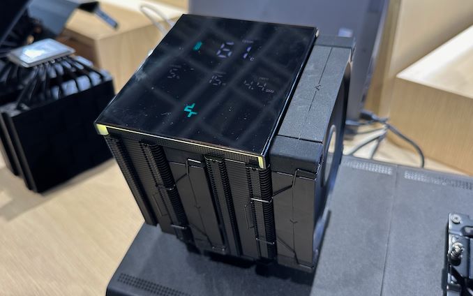

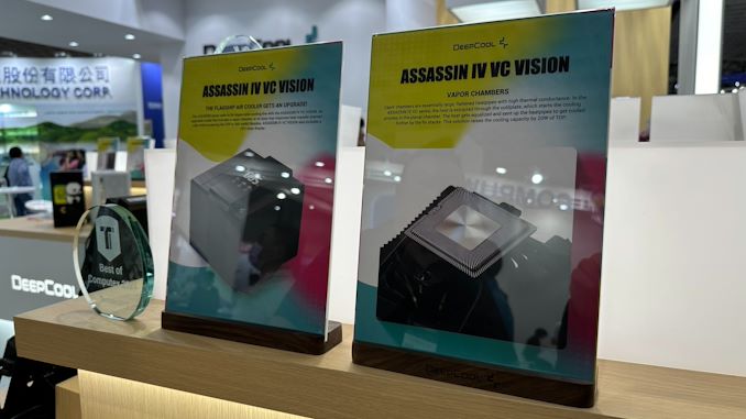
While the market for high-end CPU coolers has decidedly shifted towards closed-loop all-in-one liquid coolers over the last several years, air cooling remains alive and well. Even at the high-end, there are still further improvements and innovations being made, such as DeepCool's vapor chamber-based tower cooler, which was demonstrated at Computex.
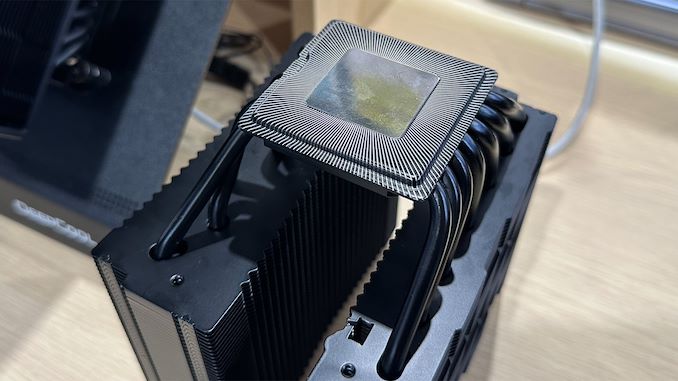
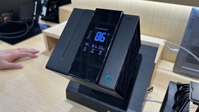
Named the Assassin IV VC Vision, DeepCool's design is an advanced concept vehicle that equips a tower cooled with both a vapor chamber in the base as well as has an LCD pad on top for extra flourish. The vapor chamber is said to increase the cooling capacity by 20W, adding a bit more of an edge to an already very powerful tower cooler design.
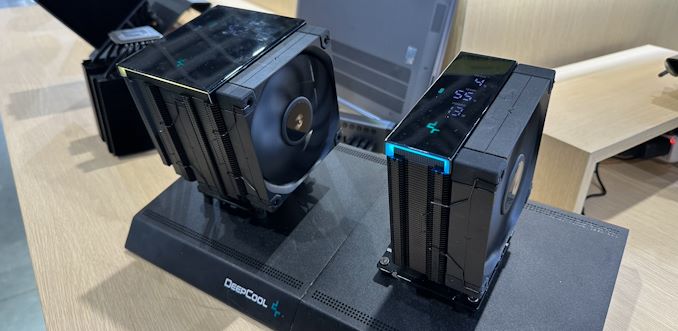
While we expect this one to come to market eventually, don't be surprised if both vapor chamber and the screen to land on other products together or separately. For example, the massive DeepCool Assassin IV VC Vision has a more compact brother that has a screen and a vapor chamber.
The unit builds on top of the already monstrous DeepCool Assassin IV that comes with seven 0.6-mm heat pipes and can mount up to three 120/140mm fans, depending on installation (one is magnetically attached). With a weight of 1.575 kilograms – almost entirely copper and aluminum – this one is already good enough to cool down even the highest-performing CPUs.
DeepCool is currently trying to figure out recommended pricing for its Assassin IV VC Vision cooler, but the original Assassin IV costs $99.99, so expect the unit with a vapor chamber and a screen to build on top of that.

Standard CPU coolers, while adequate for managing basic thermal loads, often fall short in terms of noise reduction and superior cooling efficiency. This limitation drives advanced users and system builders to seek aftermarket solutions tailored to their specific needs. The high-end aftermarket cooler market is highly competitive, with manufacturers striving to offer products with exceptional performance.
Endorfy, previously known as SilentiumPC, is a Polish manufacturer that has undergone a significant transformation to expand its presence in global markets. The brand is known for delivering high-performance cooling solutions with a strong focus on balancing efficiency and affordability. By rebranding as Endorfy, the company aims to enter premium market segments while continuing to offer reliable, high-quality cooling products.
SilentiumPC became very popular in the value/mainstream segments of the PC market with their products, the spearhead of which probably was the Fera 5 cooler that we reviewed a little over two years ago and had a remarkable value for money. Today’s review places Endorfy’s largest CPU cooler, the Fortis 5 Dual Fan, on our laboratory test bench. The Fortis 5 is the largest CPU air cooler the company currently offers and is significantly more expensive than the Fera 5, yet it still is a single-tower cooler that strives to strike a balance between value, compatibility, and performance.
Cases/Cooling/PSUs![Micron: U.S. Fabs Will Start Operating in 2026 - 2029 <p align="center"><a href="https://www.anandtech.com/show/21459/micron-u-s-fabs-will-start-operating-in-2026-2029"><img src="https://images.anandtech.com/doci/21459/micron-server-datacenter-general-generic-678_575px.jpg" alt="" /></a></p><p><p>When Micron announced plans to build two new fabs in the U.S. in 2022, the company vaguely said both would come online by the decade's end. Then, in 2023, it began to optimize its spending, which pushed production at these fabrication facilities. This week, the company outlined more precise timeframes for when its fabs in <a href="https://www.anandtech.com/show/17573/micron-breaks-ground-on-its-15-billion-euv-dram-fab-in-the-us">Idaho</a> and <a href="https://www.anandtech.com/show/17606/micron-announces-100-billion-us-fab-complex-a-20year-plan">New York</a> will start operations: this will happen from calendar 2026 to calendar 2029.</p>
<p>"<em>These fab construction investments are necessary to support supply growth for the latter half of this decade,</em>" a statement by Micron in its Q3 FY2024 financial results report <a href="https://investors.micron.com/static-files/a531c7f0-fca2-48f3-8f24-79c945aaa2d2">reads</a>. "<em>This Idaho fab will not contribute to meaningful bit supply until fiscal 2027 and the New York construction capex is not expected to contribute to bit supply growth until fiscal 2028 or later. The timing of future [wafer fab equipment] spend in these fabs will be managed to align supply growth with expected demand growth.</em>"</p>
<p>Micron's fiscal year 2027 starts in September 2026, so the new fab near Boise, Idaho, is set to start operations between September 2026 and September 2027. The company's fiscal 2028 starts in September 2027, so the fab will likely begin operations in calendar 2028 or later, probably depending on the demand for DRAM memory in the coming years. That said, Micron's U.S. memory fabs will begin operations between late 2026 and 2029, which aligns with the company's original plans. </p>
<p>Construction of the fab in Idaho is well underway. In contrast, construction of the New York facility has yet to begin as the company is working on regulatory and permitting processes in the state. </p>
<p>Micron's capital expenditure (CaPex) plan for FY2024 is approximately $8.0 billion, with a decrease in year-over-year spending on wafer fabrication equipment (WFE). In Q4 FY2024, the company will spend around $3 billion on fab construction, new wafer fab tools, and various expansions/upgrades.</p>
<p>Looking ahead to FY2025, the company plans a substantial increase in capex, targeting a mid-30s percentage of revenue to support various technological and facility advancements. In particular, it expects its quarterly CapEx to average above the $3 billion level seen in the fourth quarter of FY2024, which means that it plans to spend about $12 billion in its fiscal 2025, which begins in late September.</p>
<p>Half or more of the total CapEx increase in FY2025 (i.e., over $2 billion) will be allocated to constructing new fabs in Idaho and New York. Meanwhile, the FY2025 CapEx will significantly rise to fund high-bandwidth memory (HBM) assembly and testing and the construction of fabrication and back-end facilities. This increase also includes investments in technology transitions to meet growing demand. </p>
<p>"<em>Fab construction in Idaho is underway, and we are working diligently to complete the regulatory and permitting processes in New York,</em>" said Sanjay Mehrotra, chief executive officer of Micron, at the company's conference call with investors and financial analysts (via <a href="https://seekingalpha.com/article/4701253-micron-technology-inc-mu-q3-2024-earnings-call-transcript?source=content_type%3Areact%7Csection%3ATranscripts%7Csection_asset%3ATranscripts%7Cfirst_level_url%3Asymbol%7Cbutton%3ATitle%7Clock_status%3ANo%7Cline%3A1">SeekingAlpha</a>). "<em>This additional leading-edge greenfield capacity, along with continued technology transition investments in our Asia facilities, is required to meet long-term demand in the second half of this decade and beyond. These investments support our objective to maintain our current bit share over time and to grow our memory bit supply in line with long-term industry bit demand.</em>"</p>
</p> Memory](https://lh3.googleusercontent.com/blogger_img_proxy/AEn0k_tLzrBskywnNTiIE_wX-Qt38p5dmTer2QioqBnb8Zs1DByte1yfd1m8QGAKj_YOBLFwkD1Hpg7p-OQvU1yo-k17wJ4Ftz1_L-TKDdLrPAlbc6CNt7V1H2_Gb_Xbd_PjkmksyiIAJygqFBqVFq_O4mpFvlP_G7liwGznzyiEZyhuHGY=w72-h72-p-k-no-nu)

When Micron announced plans to build two new fabs in the U.S. in 2022, the company vaguely said both would come online by the decade's end. Then, in 2023, it began to optimize its spending, which pushed production at these fabrication facilities. This week, the company outlined more precise timeframes for when its fabs in Idaho and New York will start operations: this will happen from calendar 2026 to calendar 2029.
"These fab construction investments are necessary to support supply growth for the latter half of this decade," a statement by Micron in its Q3 FY2024 financial results report reads. "This Idaho fab will not contribute to meaningful bit supply until fiscal 2027 and the New York construction capex is not expected to contribute to bit supply growth until fiscal 2028 or later. The timing of future [wafer fab equipment] spend in these fabs will be managed to align supply growth with expected demand growth."
Micron's fiscal year 2027 starts in September 2026, so the new fab near Boise, Idaho, is set to start operations between September 2026 and September 2027. The company's fiscal 2028 starts in September 2027, so the fab will likely begin operations in calendar 2028 or later, probably depending on the demand for DRAM memory in the coming years. That said, Micron's U.S. memory fabs will begin operations between late 2026 and 2029, which aligns with the company's original plans.
Construction of the fab in Idaho is well underway. In contrast, construction of the New York facility has yet to begin as the company is working on regulatory and permitting processes in the state.
Micron's capital expenditure (CaPex) plan for FY2024 is approximately $8.0 billion, with a decrease in year-over-year spending on wafer fabrication equipment (WFE). In Q4 FY2024, the company will spend around $3 billion on fab construction, new wafer fab tools, and various expansions/upgrades.
Looking ahead to FY2025, the company plans a substantial increase in capex, targeting a mid-30s percentage of revenue to support various technological and facility advancements. In particular, it expects its quarterly CapEx to average above the $3 billion level seen in the fourth quarter of FY2024, which means that it plans to spend about $12 billion in its fiscal 2025, which begins in late September.
Half or more of the total CapEx increase in FY2025 (i.e., over $2 billion) will be allocated to constructing new fabs in Idaho and New York. Meanwhile, the FY2025 CapEx will significantly rise to fund high-bandwidth memory (HBM) assembly and testing and the construction of fabrication and back-end facilities. This increase also includes investments in technology transitions to meet growing demand.
"Fab construction in Idaho is underway, and we are working diligently to complete the regulatory and permitting processes in New York," said Sanjay Mehrotra, chief executive officer of Micron, at the company's conference call with investors and financial analysts (via SeekingAlpha). "This additional leading-edge greenfield capacity, along with continued technology transition investments in our Asia facilities, is required to meet long-term demand in the second half of this decade and beyond. These investments support our objective to maintain our current bit share over time and to grow our memory bit supply in line with long-term industry bit demand."
Memory

Kioxia's booth at FMS 2024 was a busy one with multiple technology demonstrations keeping visitors occupied. A walk-through of the BiCS 8 manufacturing process was the first to grab my attention. Kioxia and Western Digital announced the sampling of BiCS 8 in March 2023. We had touched briefly upon its CMOS Bonded Array (CBA) scheme in our coverage of Kioxial's 2Tb QLC NAND device and coverage of Western Digital's 128 TB QLC enterprise SSD proof-of-concept demonstration. At Kioxia's booth, we got more insights.

Traditionally, fabrication of flash chips involved placement of the associate logic circuitry (CMOS process) around the periphery of the flash array. The process then moved on to putting the CMOS under the cell array, but the wafer development process was serialized with the CMOS logic getting fabricated first followed by the cell array on top. However, this has some challenges because the cell array requires a high-temperature processing step to ensure higher reliability that can be detrimental to the health of the CMOS logic. Thanks to recent advancements in wafer bonding techniques, the new CBA process allows the CMOS wafer and cell array wafer to be processed independently in parallel and then pieced together, as shown in the models above.

The BiCS 8 3D NAND incorporates 218 layers, compared to 112 layers in BiCS 5 and 162 layers in BiCS 6. The company decided to skip over BiCS 7 (or, rather, it was probably a short-lived generation meant as an internal test vehicle). The generation retains the four-plane charge trap structure of BiCS 6. In its TLC avatar, it is available as a 1 Tbit device. The QLC version is available in two capacities - 1 Tbit and 2 Tbit.
Kioxia also noted that while the number of layers (218) doesn't compare favorably with the latest layer counts from the competition, its lateral scaling / cell shrinkage has enabled it to be competitive in terms of bit density as well as operating speeds (3200 MT/s). For reference, the latest shipping NAND from Micron - the G9 - has 276 layers with a bit density in TLC mode of 21 Gbit/mm2, and operates at up to 3600 MT/s. However, its 232L NAND operates only up to 2400 MT/s and has a bit density of 14.6 Gbit/mm2.
It must be noted that the CBA hybrid bonding process has advantages over the current processes used by other vendors - including Micron's CMOS under array (CuA) and SK hynix's 4D PUC (periphery-under-chip) developed in the late 2010s. It is expected that other NAND vendors will also move eventually to some variant of the hybrid bonding scheme used by Kioxia.
Storage
Lorem Ipsum is simply dummy text of the printing and typesetting industry. Lorem Ipsum has been the industry's.


. With a weight of 1.575 kilograms – almost entirely copper and aluminum – this one is already good enough to cool down even the highest-performing CPUs.</p>
<p style="text-align: center;"><a href="https://www.anandtech.com/show/21450/deepcool-adds-vapor-chamber-to-an-air-cooler-aio-like-performance-at-air-cooler-reliability"><img alt="" src="https://images.anandtech.com/doci/21450/IMG_1026-compact_575px.jpg" /></a></p>
<p>DeepCool is currently trying to figure out recommended pricing for its Assassin IV VC Vision cooler, but the original Assassin IV costs <a href="https://target.georiot.com/Proxy.ashx?tsid=45726&GR_URL=https%3A%2F%2Famazon.com%2FDeepCool-Assassin%2Fdp%2FB0CC2QNF73%3Ftag%3Dhawk-future-20%26ascsubtag%3Danandtech-us-2038795906289287965-20">$99.99</a>, so expect the unit with a vapor chamber and a screen to build on top of that.</p>
<p style="text-align: center;"><a href="https://www.anandtech.com/show/21450/deepcool-adds-vapor-chamber-to-an-air-cooler-aio-like-performance-at-air-cooler-reliability"><img alt="" src="https://images.anandtech.com/doci/21450/description_575px.jpg" /></a></p>
</p> Cases/Cooling/PSUs)
. With a weight of 1.575 kilograms – almost entirely copper and aluminum – this one is already good enough to cool down even the highest-performing CPUs.</p>
<p style="text-align: center;"><a href="https://www.anandtech.com/show/21450/deepcool-adds-vapor-chamber-to-an-air-cooler-aio-like-performance-at-air-cooler-reliability"><img alt="" src="https://images.anandtech.com/doci/21450/IMG_1026-compact_575px.jpg" /></a></p>
<p>DeepCool is currently trying to figure out recommended pricing for its Assassin IV VC Vision cooler, but the original Assassin IV costs <a href="https://target.georiot.com/Proxy.ashx?tsid=45726&GR_URL=https%3A%2F%2Famazon.com%2FDeepCool-Assassin%2Fdp%2FB0CC2QNF73%3Ftag%3Dhawk-future-20%26ascsubtag%3Danandtech-us-2038795906289287965-20">$99.99</a>, so expect the unit with a vapor chamber and a screen to build on top of that.</p>
<p style="text-align: center;"><a href="https://www.anandtech.com/show/21450/deepcool-adds-vapor-chamber-to-an-air-cooler-aio-like-performance-at-air-cooler-reliability"><img alt="" src="https://images.anandtech.com/doci/21450/description_575px.jpg" /></a></p>
</p> Cases/Cooling/PSUs | https://compbuddey.blogspot.com/2024/07/deepcool-adds-vapor-chamber-to-air_12.html)
. With a weight of 1.575 kilograms – almost entirely copper and aluminum – this one is already good enough to cool down even the highest-performing CPUs.</p>
<p style="text-align: center;"><a href="https://www.anandtech.com/show/21450/deepcool-adds-vapor-chamber-to-an-air-cooler-aio-like-performance-at-air-cooler-reliability"><img alt="" src="https://images.anandtech.com/doci/21450/IMG_1026-compact_575px.jpg" /></a></p>
<p>DeepCool is currently trying to figure out recommended pricing for its Assassin IV VC Vision cooler, but the original Assassin IV costs <a href="https://target.georiot.com/Proxy.ashx?tsid=45726&GR_URL=https%3A%2F%2Famazon.com%2FDeepCool-Assassin%2Fdp%2FB0CC2QNF73%3Ftag%3Dhawk-future-20%26ascsubtag%3Danandtech-us-2038795906289287965-20">$99.99</a>, so expect the unit with a vapor chamber and a screen to build on top of that.</p>
<p style="text-align: center;"><a href="https://www.anandtech.com/show/21450/deepcool-adds-vapor-chamber-to-an-air-cooler-aio-like-performance-at-air-cooler-reliability"><img alt="" src="https://images.anandtech.com/doci/21450/description_575px.jpg" /></a></p>
</p> Cases/Cooling/PSUs&body=https://compbuddey.blogspot.com/2024/07/deepcool-adds-vapor-chamber-to-air_12.html)
0 Comments