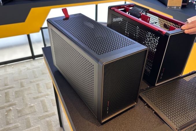

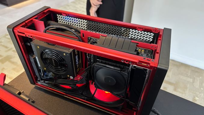
With the highly integrated nature of PCs these days, the Mini-ITX form-factor has become a very viable option for high-performance gaming system. With plenty of motherboards available for both AMD and Intel's latest platforms, equipping an ITX system with a CPU is easy enough. But the small size of the form factor means that housing an ultra-wide flagship-level graphics card remains an issue. For this year's Computex trade show, Antec was showing off their solution to the problem of giant video cards: the Performance 1M case, a Mini-ITX case with a separate chamber just for a large video card.
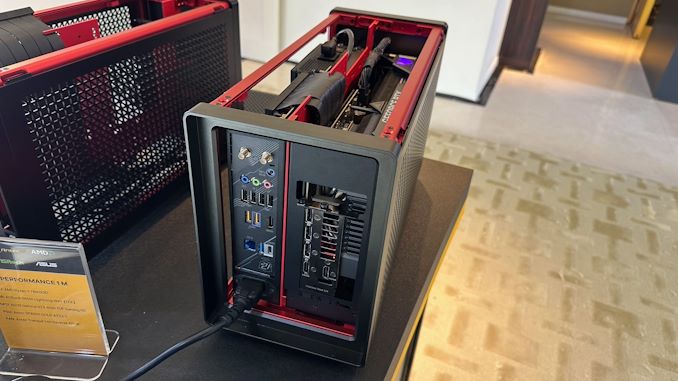
Antec's Performance 1M is a dual-chamber Mini-ITX chassis that splits off the video card from the rest of the system. The primary chamber houses a Mini-ITX motherboard and an SFX power supply, while the secondary chamber houses a huge graphics card. Notably, the two chambers are bridged using a PCIe riser cable, allowing the motherboard chamber to be far shorter than even a half-height PCIe card, while the video card chamber can hold a triple-slot video card parallel to the motherboard chamber, cutting down on wasted space. For Antec's Computex demo, the company had a triple-slot ASUS GeForce RTX 4090 installed to showcase how this worked.
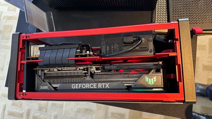
Antec's decision to allocate most of the case's volume to th video card chamber does come with a slight catch, however: it doesn't leave much space for a CPU cooler in the motherboard chamber. The short motherboard chamber means that system builders will have to use a low-profile cooler; these are readily available, but it does leave less thermal headroom overall for high-end CPUs. So there are still trade-offs for being able to accommodate a high-end video card.
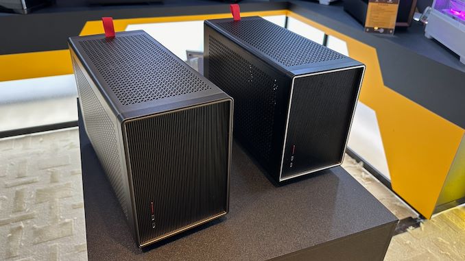
Otherwise, the Performance 1M chassis from Antec look very stylish and are traditionally well built from stainless steel and aluminum. The chassis can be equipped with two 120-mm or two 140-mm coolers for extra airflow (which will help performance), one 2.5-inch SATA SSD, and even some RGB bling. To make the PC built inside a Performance 1M case more convenient to use, there are two USB Type-C ports on the front.
Of course, housing a GeForce RTX 4090 graphics card in a Mini-ITX chassis has its peculiarities when it comes to dimensions and Antec's Performance 1M measures 424×175×260mm, which is pretty large. On the other hand, for an ultra-high-performance gaming system, this is pretty compact.
Antec's Performance 1M Mini-ITX chassis will be available in gunmetal gray and matte black colors sometimes later this year. Pricing is something that the company is thinking about now, though keep in mind that we are talking about unique premium products.
Cases/Cooling/PSUs
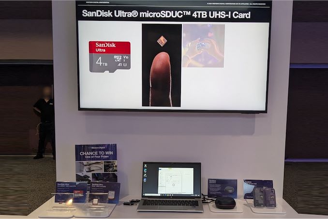
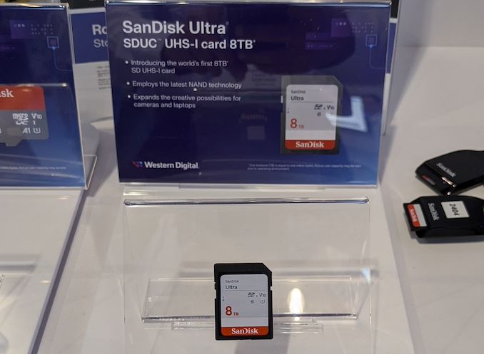
Western Digital's BiCS8 218-layer 3D NAND is being put to good use in a wide range of client and enterprise platforms, including WD's upcoming Gen 5 client SSDs and 128 TB-class datacenter SSD. On the external storage front, the company demonstrated four different products: for card-based media, 4 TB microSDUC and 8 TB SDUC cards with UHS-I speeds, and on the portable SSD front we had two 16 TB drives. One will be a SanDisk Desk Drive with external power, and the other in the SanDisk Extreme Pro housing with a lanyard opening in the case.
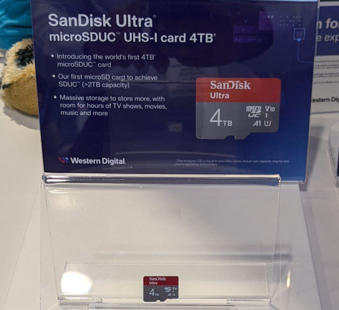
All of these are using BiCS8 QLC NAND, though I did hear booth talk (as I was taking leave) that they were not supposed to divulge the use of QLC in these products. The 4 TB microSDUC and 8 TB SDUC cards are rated for UHS-I speeds. They are being marketed under the SanDisk Ultra branding.
The SanDisk Desk Drive is an external SSD with a 18W power adapter, and it has been in the market for a few months now. Initially launched in capacities up to 8 TB, Western Digital had promised a 16 TB version before the end of the year. It appears that the product is coming to retail quite soon. One aspect to note is that this drive has been using TLC for the SKUs that are currently in the market, so it appears unlikely that the 16 TB version would be QLC. The units (at least up to the 8 TB capacity point) come with two SN850XE drives. Given the recent introduction of the 8 TB SN850X, an 'E' version with tweaked firmware is likely to be present in the 16 TB Desk Drive.
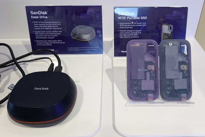
The 16 TB portable SSD in the SanDisk Extreme housing was a technology demonstration. It is definitely the highest capacity bus-powered portable SSD demonstrated by any vendor at any trade show thus far. Given the 16 TB Desk Drive's imminent market introduction, it is just a matter of time before the technology demonstration of the bus-powered version becomes a retail reality.
Storage

A few years back, the Japanese government's New Energy and Industrial Technology Development Organization (NEDO ) allocated funding for the development of green datacenter technologies. With the aim to obtain up to 40% savings in overall power consumption, several Japanese companies have been developing an optical interface for their enterprise SSDs. And at this year's FMS, Kioxia had their optical interface on display.

For this demonstration, Kioxia took its existing CM7 enterprise SSD and created an optical interface for it. A PCIe card with on-board optics developed by Kyocera is installed in the server slot. An optical interface allows data transfer over long distances (it was 40m in the demo, but Kioxia promises lengths of up to 100m for the cable in the future). This allows the storage to be kept in a separate room with minimal cooling requirements compared to the rack with the CPUs and GPUs. Disaggregation of different server components will become an option as very high throughput interfaces such as PCIe 7.0 (with 128 GT/s rates) become available.

The demonstration of the optical SSD showed a slight loss in IOPS performance, but a significant advantage in the latency metric over the shipping enterprise SSD behind a copper network link. Obviously, there are advantages in wiring requirements and signal integrity maintenance with optical links.
Being a proof-of-concept demonstration, we do see the requirement for an industry-standard approach if this were to gain adoption among different datacenter vendors. The PCI-SIG optical workgroup will need to get its act together soon to create a standards-based approach to this problem.
Storage

Under the CHIPS & Science Act, the U.S. government provided tens of billions of dollars in grants and loans to the world's leading maker of chips, such as Intel, Samsung, and TSMC, which will significantly expand the country's semiconductor production industry in the coming years. However, most chips are typically tested, assembled, and packaged in Asia, which has left the American supply chain incomplete. Addressing this last gap in the government's domestic chip production plans, these past couple of weeks the U.S. government signed memorandums of understanding worth about $1.5 billion with Amkor and SK hynix to support their efforts to build chip packaging facilities in the U.S.
Amkor plans to build a $2 billion advanced packaging facility near Peoria, Arizona, to test and assemble chips produced by TSMC at its Fab 21 near Phoenix, Arizona. The company signed a MOU that offers $400 million in direct funding and access to $200 million in loans under the CHIPS & Science Act. In addition, the company plans to take advantage of a 25% investment tax credit on eligible capital expenditures.
Set to be strategically positioned near TSMC's upcoming Fab 21 complex in Arizona, Amkor's Peoria facility will occupy 55 acres and, when fully completed, will feature over 500,000 square feet (46,451 square meters) of cleanroom space, more than twice the size of Amkor's advanced packaging site in Vietnam. Although the company has not disclosed the exact capacity or the specific technologies the facility will support, it is expected to cater to a wide range of industries, including automotive, high-performance computing, and mobile technologies. This suggests the new plant will offer diverse packaging solutions, including traditional, 2.5D, and 3D technologies.
Amkor has collaborated extensively with Apple on the vision and initial setup of the Peoria facility, as Apple is slated to be the facility's first and largest customer, marking a significant commitment from the tech giant. This partnership highlights the importance of the new facility in reinforcing the U.S. semiconductor supply chain and positioning Amkor as a key partner for companies relying on TSMC's manufacturing capabilities. The project is expected to generate around 2,000 jobs and is scheduled to begin operations in 2027.
This week SK hynix also signed a preliminary agreement with the U.S. government to receive up to $450 million in direct funding and $500 million in loans to build an advanced memory packaging facility in West Lafayette, Indiana.
The proposed facility is scheduled to begin operations in 2028, which means that it will assemble HBM4 or HBM4E memory. Meanwhile, DRAM devices for high bandwidth memory (HBM) stacks will still be produced in South Korea. Nonetheless, packing finished HBM4/HBM4E in the U.S. and possibly integrating these memory modules with high-end processors is a big deal.
In addition to building its packaging plant, SK hynix plans to collaborate with Purdue University and other local research institutions to advance semiconductor technology and packaging innovations. This partnership is intended to bolster research and development in the region, positioning the facility as a hub for AI technology and skilled employment.
Semiconductors
Lorem Ipsum is simply dummy text of the printing and typesetting industry. Lorem Ipsum has been the industry's.


, one 2.5-inch SATA SSD, and even some RGB bling. To make the PC built inside a Performance 1M case more convenient to use, there are two USB Type-C ports on the front.</p>
<p><a href="https://www.anandtech.com/show/21443/antecs-miniitx-chassis-can-house-a-geforce-rtx-4090"><img alt="" src="https://images.anandtech.com/doci/21443/IMG_0846_575px.jpg" /></a></p>
<p>Of course, housing a GeForce RTX 4090 graphics card in a Mini-ITX chassis has its peculiarities when it comes to dimensions and Antec's Performance 1M measures 424×175×260mm, which is pretty large. On the other hand, for an ultra-high-performance gaming system, this is pretty compact.</p>
<p style="text-align: center;"><a href="https://www.anandtech.com/show/21443/antecs-miniitx-chassis-can-house-a-geforce-rtx-4090"><img alt="" src="https://images.anandtech.com/doci/21443/IMG_0850_575px.jpg" /></a></p>
<p>Antec's Performance 1M Mini-ITX chassis will be available in gunmetal gray and matte black colors sometimes later this year. Pricing is something that the company is thinking about now, though keep in mind that we are talking about unique premium products.</p>
</p> Cases/Cooling/PSUs)
, one 2.5-inch SATA SSD, and even some RGB bling. To make the PC built inside a Performance 1M case more convenient to use, there are two USB Type-C ports on the front.</p>
<p><a href="https://www.anandtech.com/show/21443/antecs-miniitx-chassis-can-house-a-geforce-rtx-4090"><img alt="" src="https://images.anandtech.com/doci/21443/IMG_0846_575px.jpg" /></a></p>
<p>Of course, housing a GeForce RTX 4090 graphics card in a Mini-ITX chassis has its peculiarities when it comes to dimensions and Antec's Performance 1M measures 424×175×260mm, which is pretty large. On the other hand, for an ultra-high-performance gaming system, this is pretty compact.</p>
<p style="text-align: center;"><a href="https://www.anandtech.com/show/21443/antecs-miniitx-chassis-can-house-a-geforce-rtx-4090"><img alt="" src="https://images.anandtech.com/doci/21443/IMG_0850_575px.jpg" /></a></p>
<p>Antec's Performance 1M Mini-ITX chassis will be available in gunmetal gray and matte black colors sometimes later this year. Pricing is something that the company is thinking about now, though keep in mind that we are talking about unique premium products.</p>
</p> Cases/Cooling/PSUs | https://compbuddey.blogspot.com/2024/07/antecs-performance-1m-mini-itx-chassis_9.html)
, one 2.5-inch SATA SSD, and even some RGB bling. To make the PC built inside a Performance 1M case more convenient to use, there are two USB Type-C ports on the front.</p>
<p><a href="https://www.anandtech.com/show/21443/antecs-miniitx-chassis-can-house-a-geforce-rtx-4090"><img alt="" src="https://images.anandtech.com/doci/21443/IMG_0846_575px.jpg" /></a></p>
<p>Of course, housing a GeForce RTX 4090 graphics card in a Mini-ITX chassis has its peculiarities when it comes to dimensions and Antec's Performance 1M measures 424×175×260mm, which is pretty large. On the other hand, for an ultra-high-performance gaming system, this is pretty compact.</p>
<p style="text-align: center;"><a href="https://www.anandtech.com/show/21443/antecs-miniitx-chassis-can-house-a-geforce-rtx-4090"><img alt="" src="https://images.anandtech.com/doci/21443/IMG_0850_575px.jpg" /></a></p>
<p>Antec's Performance 1M Mini-ITX chassis will be available in gunmetal gray and matte black colors sometimes later this year. Pricing is something that the company is thinking about now, though keep in mind that we are talking about unique premium products.</p>
</p> Cases/Cooling/PSUs&body=https://compbuddey.blogspot.com/2024/07/antecs-performance-1m-mini-itx-chassis_9.html)
0 Comments