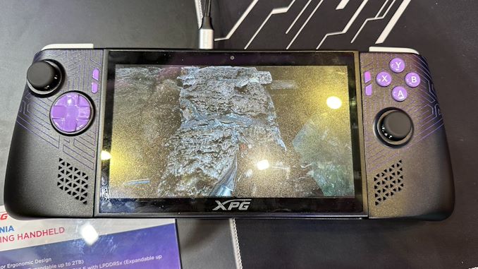

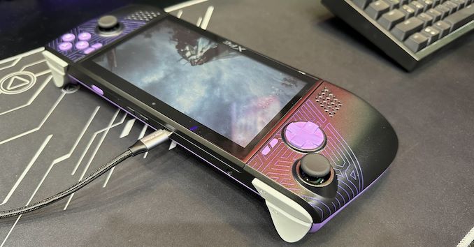
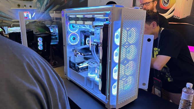
With the rise of the handheld gaming PC market, we've seen PC vendors and their partners toy with a number of tricks and tweaks to improve improve framerates in games, with some of their latest efforts on display at this year's Computex trade show. Perhaps the most interesting find thus far comes from ADATA sub-brand XPG, who is demoing their prototype "Nia" handheld PC, which uses eye tracking and dynamic foveated rendering to further improve their rendering performance.
For those unfamiliar, dynamic foveated rendering is a graphics technique that is sometimes used to boost performance in virtual reality (VR) and augmented reality (AR) applications by taking advantage of how human vision works. Typically, humans can only perceive detailed imagery in the relatively small central area of our vision called the fovea, while our peripheral vision is much less detailed. Dynamic foveated rendering, in turn, exploits this by using real-time eye tracking to determine where the user is looking, and then rendering just that area in high/full resolution, while rendering the peripheral areas in lower resolution. The net result is that only a fraction of the screen is rendered at full detail, which cuts down on the total amount of rendering work required and boosting framerates on performance-limited devices.
As stated before, this technology is sometimes used in high-end AR/VR headsets, where high resolution displays are placed mere inches from one's face. This ends up being an ideal use case for the technique, since at those distances, only a small fraction of the screen is within the fovea.
Using dynamic foveated rendering for a handheld, on the other hand, is a more novel application. All of the same visual principles apply, but the resolutions at play are lower, and the screen is farther from the users' eyes. This makes a handheld device a less ideal use case, at least on paper, as a larger portion of the screen is going to be in the fovea, and thus will need to be rendered at full resolution. None the less, it will be interesting to see how XPG's efforts pan out, and if dynamic foveated rendering is beneficial enough for handheld PCs. As we sometimes see with trade show demos, not everything makes it out of the prototype stage.
According to a press release put out by ADATA ahead of the trade show, the eye tracking technology is being provided by AMD collaborator Eyeware. Notably, their software-based approach runs on top of standard webcams, rather than requiring IR cameras. So the camera hardware itself should be pretty straight-forward.
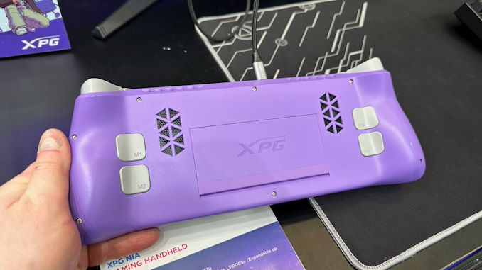
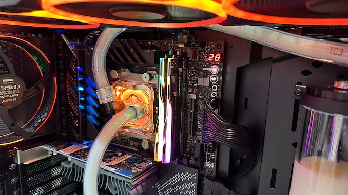
Foveated rendering aside, XPG is making sure that the Nia won't be a one-trick pony. The handheld's other major claim to fame is its hardware swappability. The prototype handheld not only features a removable M.2-2230 SSD, but the company is also taking advantage of the recently-introduced LPCAMM2 memory module standard to introduce removable DRAM. Via a hatch in the back of the handheld, device owners would be able to swap out LPCAMM2 LPDDR5X modules for higher capacity versions. This would give the handheld an additional degree of future-proofness over current handhelds, which use non-replaceable soldered-down memory.
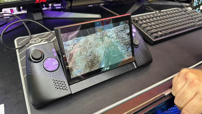
Rounding out the package, the current prototype is based on an AMD's Zen 4 Phoenix APU, which is used across both of the company's current mobile lines (Ryzen Mobile 7000/8000 and Ryzen Z1). Meanwhile, the unit's display is adjustable, allowing it to be angled away from the body of the handheld.
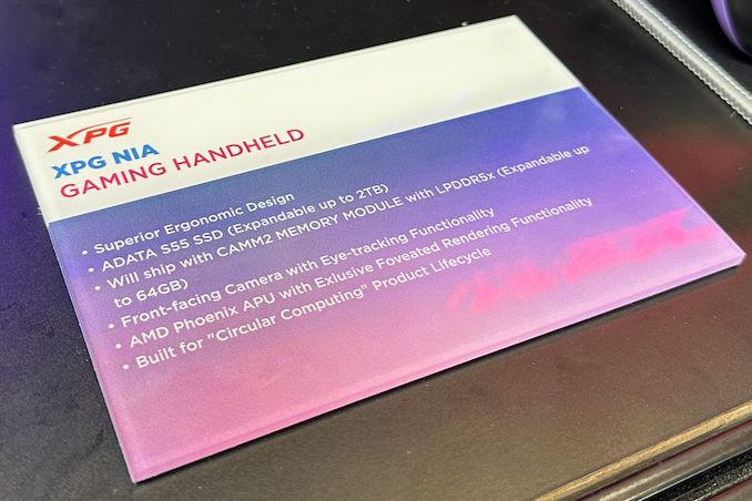
Assuming all goes well with the prototype, XPG aims to release a finished product in 2025.

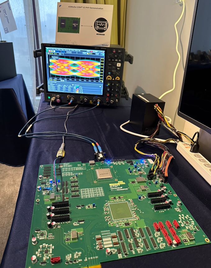
The USB Implementers Forum (USB-IF) introduced USB4 version 2.0 in fall 2022, and it expects systems and devices with the tech to emerge later this year and into next year. These upcoming products will largely rely on Intel's Barlow Ridge controller, a full-featured Thunderbolt 5 controller that goes above and beond the baseline USB4 v2 spec. And though extremely capable, Intel's Thunderbolt controllers are also quite expensive, and Barlow Ridge isn't expected to be any different. Fortunately, for system and device vendors that just need a basic USB4 v2 solution, ASMedia is also working on its own USB4 v2 controller.
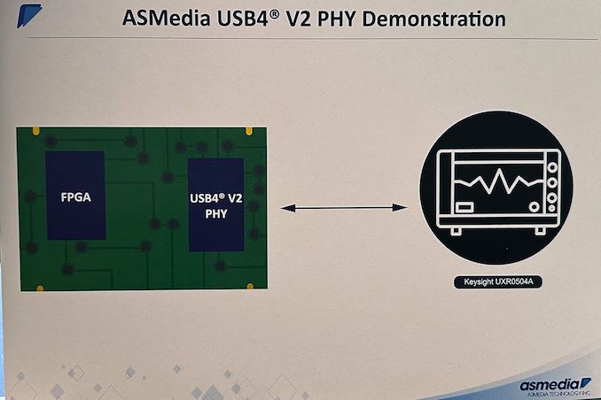
At Computex 2024, ASMedia demonstrated a prototype of its upcoming USB4 v2 physical interface (PHY), which will support USB4 v2's new Gen 4 (160Gbps) data rates and the associated PAM-3 signal encoding. The prototype was implemented using an FPGA, as the company yet has to tape out the completed controller.
Ultimately, the purpose of showing off a FPGA-based PHY at Computex was to allow ASMedia to demonstrate their current PHY design. With the shift to PAM-3 encoding for USB4 v2, ASMedia (and the rest of the USB ecosystem) must develop significantly more complex controllers – and there's no part of that more critical than a solid and reliable PHY design.
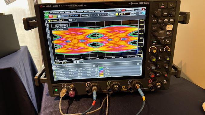
As part of their demonstration, ASMedia had a classic eye diagram display. The eye diagram demoed has a clear opening in the center, which is indicative of good signal integrity, as the larger the eye opening, the less distortion and noise in the signal. The horizontal width of the eye opening represents the time window in which the signal can be sampled correctly, so the relatively narrow horizontal spread of the eye opening suggests that there is minimal jitter, meaning the signal transitions are consistent and predictable. Finally, the vertical height of the eye opening indicates the signal amplitude and the rather tall eye opening suggests a higher signal-to-noise ratio (SNR), meaning that the signal is strong compared to any noise present.
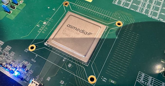
ASMedia itself is one of the major suppliers for discrete USB controllers, so the availability of ASMedia's USB4 v2 chip is crucial for adoption of the standard in general. While Intel will spearhead the industry with their Barlow Ridge Thunderbolt 5/USB4 v2 controller, ASMedia's controller is poised to end up in a far larger range of devices. So the importance of the company's USB4 v2 PHY demo is hard to overstate.
Demos aside, ASMedia is hoping to tape the chip out soon. If all goes well, the company expects their first USB4 v2 controllers to hit the market some time in the second half of 2025.
The USB Implementers Forum (USB-IF) introduced USB4 version 2.0 in fall 2022, and it expects systems and devices with the tech to emerge later this year and into next year. These upcoming products will largely rely on Intel's Barlow Ridge controller, a full-featured Thunderbolt 5 controller that goes above and beond the baseline USB4 v2 spec. And though extremely capable, Intel's Thunderbolt controllers are also quite expensive, and Barlow Ridge isn't expected to be any different. Fortunately, for system and device vendors that just need a basic USB4 v2 solution, ASMedia is also working on its own USB4 v2 controller.
At Computex 2024, ASMedia demonstrated a prototype of its upcoming USB4 v2 physical interface (PHY), which will support USB4 v2's new Gen 4 (160Gbps) data rates and the associated PAM-3 signal encoding. The prototype was implemented using an FPGA, as the company yet has to tape out the completed controller.
Ultimately, the purpose of showing off a FPGA-based PHY at Computex was to allow ASMedia to demonstrate their current PHY design. With the shift to PAM-3 encoding for USB4 v2, ASMedia (and the rest of the USB ecosystem) must develop significantly more complex controllers – and there's no part of that more critical than a solid and reliable PHY design.
As part of their demonstration, ASMedia had a classic eye diagram display. The eye diagram demoed has a clear opening in the center, which is indicative of good signal integrity, as the larger the eye opening, the less distortion and noise in the signal. The horizontal width of the eye opening represents the time window in which the signal can be sampled correctly, so the relatively narrow horizontal spread of the eye opening suggests that there is minimal jitter, meaning the signal transitions are consistent and predictable. Finally, the vertical height of the eye opening indicates the signal amplitude and the rather tall eye opening suggests a higher signal-to-noise ratio (SNR), meaning that the signal is strong compared to any noise present.
ASMedia itself is one of the major suppliers for discrete USB controllers, so the availability of ASMedia's USB4 v2 chip is crucial for adoption of the standard in general. While Intel will spearhead the industry with their Barlow Ridge Thunderbolt 5/USB4 v2 controller, ASMedia's controller is poised to end up in a far larger range of devices. So the importance of the company's USB4 v2 PHY demo is hard to overstate.
Demos aside, ASMedia is hoping to tape the chip out soon. If all goes well, the company expects their first USB4 v2 controllers to hit the market some time in the second half of 2025.

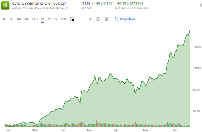
Thanks to the success of the burgeoning market for AI accelerators, NVIDIA has been on a tear this year. And the only place that’s even more apparent than the company’s rapidly growing revenues is in the company’s stock price and market capitalization. After breaking into the top 5 most valuable companies only earlier this year, NVIDIA has reached the apex of Wall Street, closing out today as the world’s most valuable company.
With a closing price of $135.58 on a day that saw NVIDIA’s stock pop up another 3.5%, NVIDIA has topped both Microsoft and Apple in valuation, reaching a market capitalization of $3.335 trillion. This follows a rapid rise in the company’s stock price, which has increased by 47% in the last month alone – particularly on the back of NVIDIA’s most recent estimates-beating earnings report – as well as a recent 10-for-1 stock split. And looking at the company’s performance over a longer time period, NVIDIA’s stock jumped a staggering 218% over the last year, or a mere 3,474% over the last 5 years.
NVIDIA’s ascension continues a trend over the last several years of tech companies all holding the top spots in the market capitalization rankings. Though this is the first time in quite a while that the traditional tech leaders of Apple and Microsoft have been pushed aside.
| Market Capitalization Rankings | ||
| Market Cap | Stock Price | |
| NVIDIA | $3.335T | $135.58 |
| Microsoft | $3.317T | $446.34 |
| Apple | $3.285T | $214.29 |
| Alphabet | $2.170T | $176.45 |
| Amazon | $1.902T | $182.81 |
Driving the rapid growth of NVIDIA and its market capitalization has been demand for AI accelerators from NVIDIA, particularly the company’s server-grade H100, H200, and GH200 accelerators for AI training. As the demand for these products has spiked, NVIDIA has been scaling up accordingly, repeatedly beating market expectations for how many of the accelerators they can ship – and what price they can charge. And despite all that growth, orders for NVIDIA’s high-end accelerators are still backlogged, underscoring how NVIDIA still isn’t meeting the full demands of hyperscalers and other enterprises.
Consequently, NVIDIA’s stock price and market capitalization have been on a tear on the basis of these future expectations. With a price-to-earnings (P/E) ratio of 76.7 – more than twice that of Microsoft or Apple – NVIDIA is priced more like a start-up than a 30-year-old tech company. But then it goes without saying that most 30-year-old tech companies aren’t tripling their revenue in a single year, placing NVIDIA in a rather unique situation at this time.
Like the stock market itself, market capitalizations are highly volatile. And historically speaking, it’s far from guaranteed that NVIDIA will be able to hold the top spot for long, never mind day-to-day fluctuations. NVIDIA, Apple, and Microsoft’s valuations are all within $50 billion (1.%) of each other, so for the moment at least, it’s still a tight race between all three companies. But no matter what happens from here, NVIDIA gets the exceptionally rare claim of having been the most valuable company in the world at some point.
(Carousel image courtesy MSN Money)
GPUs

Kioxia's booth at FMS 2024 was a busy one with multiple technology demonstrations keeping visitors occupied. A walk-through of the BiCS 8 manufacturing process was the first to grab my attention. Kioxia and Western Digital announced the sampling of BiCS 8 in March 2023. We had touched briefly upon its CMOS Bonded Array (CBA) scheme in our coverage of Kioxial's 2Tb QLC NAND device and coverage of Western Digital's 128 TB QLC enterprise SSD proof-of-concept demonstration. At Kioxia's booth, we got more insights.

Traditionally, fabrication of flash chips involved placement of the associate logic circuitry (CMOS process) around the periphery of the flash array. The process then moved on to putting the CMOS under the cell array, but the wafer development process was serialized with the CMOS logic getting fabricated first followed by the cell array on top. However, this has some challenges because the cell array requires a high-temperature processing step to ensure higher reliability that can be detrimental to the health of the CMOS logic. Thanks to recent advancements in wafer bonding techniques, the new CBA process allows the CMOS wafer and cell array wafer to be processed independently in parallel and then pieced together, as shown in the models above.

The BiCS 8 3D NAND incorporates 218 layers, compared to 112 layers in BiCS 5 and 162 layers in BiCS 6. The company decided to skip over BiCS 7 (or, rather, it was probably a short-lived generation meant as an internal test vehicle). The generation retains the four-plane charge trap structure of BiCS 6. In its TLC avatar, it is available as a 1 Tbit device. The QLC version is available in two capacities - 1 Tbit and 2 Tbit.
Kioxia also noted that while the number of layers (218) doesn't compare favorably with the latest layer counts from the competition, its lateral scaling / cell shrinkage has enabled it to be competitive in terms of bit density as well as operating speeds (3200 MT/s). For reference, the latest shipping NAND from Micron - the G9 - has 276 layers with a bit density in TLC mode of 21 Gbit/mm2, and operates at up to 3600 MT/s. However, its 232L NAND operates only up to 2400 MT/s and has a bit density of 14.6 Gbit/mm2.
It must be noted that the CBA hybrid bonding process has advantages over the current processes used by other vendors - including Micron's CMOS under array (CuA) and SK hynix's 4D PUC (periphery-under-chip) developed in the late 2010s. It is expected that other NAND vendors will also move eventually to some variant of the hybrid bonding scheme used by Kioxia.
Storage
UPDATE 6/12: Micron notified us that it expects its HBM market share to rise to mid-20% in the middle of calendar 2025, not in the middle of fiscal 2025.
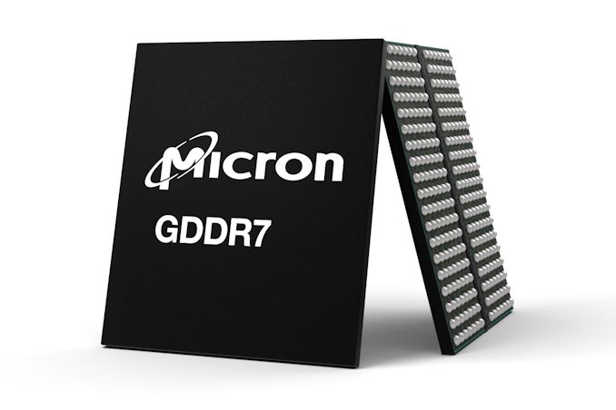
For Computex week, Micron was at the show in force in order to talk about its latest products across the memory spectrum. The biggest news for the memory company was that it has kicked-off sampling of it's next-gen GDDR7 memory, which is expected to start showing up in finished products later this year and was being demoed on the show floor. Meanwhile, the company is also eyeing taking a much larger piece of the other pillar of the high-performance memory market – High Bandwidth Memory – with aims of capturing around 25% of the premium HBM market.
Micron's first GDDR7 chip is a 16 Gb memory device with a 32 GT/sec (32Gbps/pin) transfer rate, which is significantly faster than contemporary GDDR6/GDDR6X. As outlined with JEDEC's announcement of GDDR7 earlier this year, the latest iteration of the high-performance memory technology is slated to improve on both memory bandwidth and capacity, with bandwidths starting at 32 GT/sec and potentially climbing another 50% higher to 48 GT/sec by the time the technology reaches its apex. And while the first chips are starting off at the same 2GByte (16Gbit) capacity as today's GDDR6(X) chips, the standard itself defines capacities as high as 64Gbit.
Of particular note, GDDR7 brings with it the switch to PAM3 (3-state) signal encoding, moving from the industry's long-held NRZ (2-state) signaling. As Micron was responsible for the bespoke GDDR6X technology, which was the first major DRAM spec to use PAM signaling (in its case, 4-state PAM4), Micron reckons they have a leg-up with GDDR7 development, as they're already familiar with working with PAM.
The GDDR7 transition also brings with it a change in how chips are organized, with the standard 32-bit wide chip now split up into four 8-bit sub-channels. And, like most other contemporary memory standards, GDDR7 is adding on-die ECC support to hold the line on chip reliability (though as always, we should note that on-die ECC isn't meant to be a replacement for full, multi-chip ECC). The standard also implements some other RAS features such as error checking and scrubbing, which although are not germane to gaming, will be a big deal for compute/AI use cases.
The added complexity of GDDR7 means that the pin count is once again increasing as well, with the new standard adding a further 86 pins to accommodate the data transfer and power delivery changes, bringing it to a total of 266 pins. With that said, the actual package size is remaining unchanged from GDDR5/GDDR6, maintaining that familiar 14mm x 12mm package. Memory manufacturers are instead using smaller diameter balls, as well as decreasing the pitch between the individual solder balls – going from GDDR6's 0.75mm x 0.75mm pitch to a slightly shorter 0.75mm x 0.73mm pitch. This allows the same package to fit in another 5 rows of contacts.
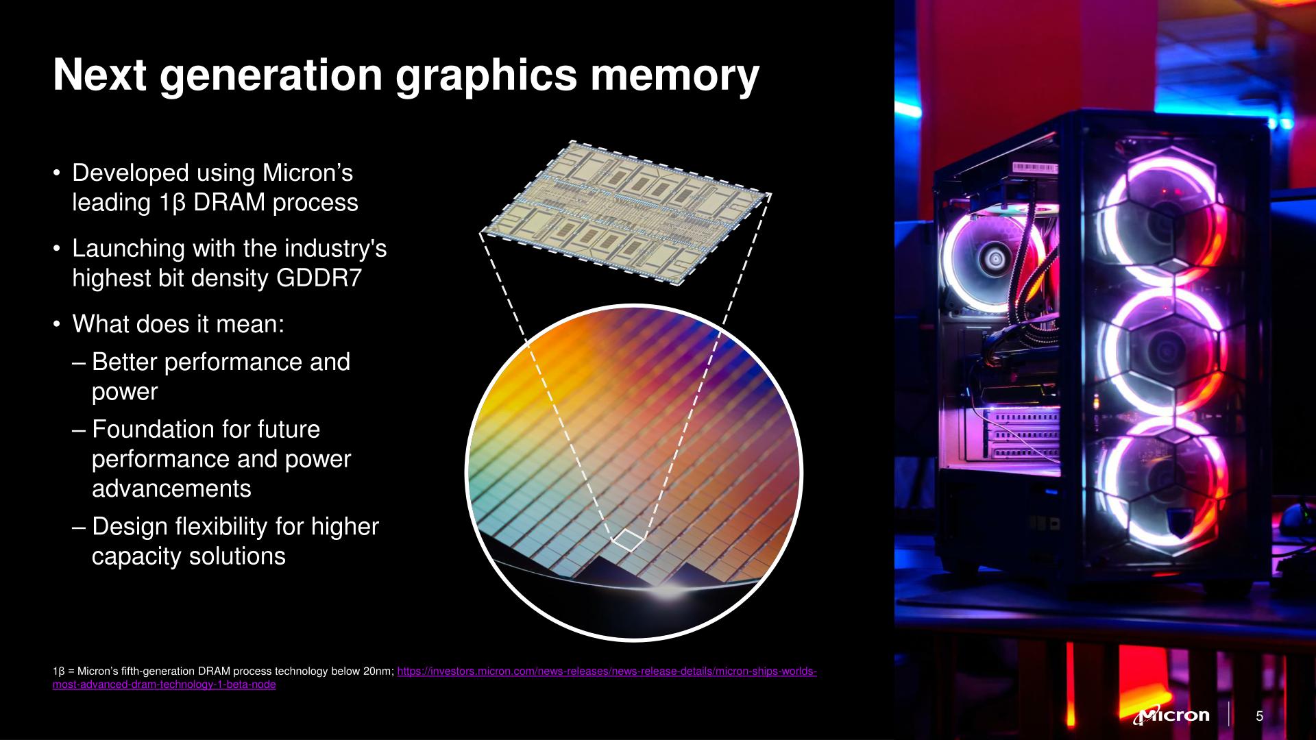
As for Micron's own production plans, the company is using its latest 1-beta (1β) fabrication process. While the major memory manufacturers don't readily publish the physical parameters of their processes these days, Micron believes that they have the edge on density with 1β, and consequently will be producing the densest GDDR7 at launch. And, while more nebulous, the company company believes that 1β will give them an edge in power efficiency as well.
Micron says that the first devices incorporating GDDR7 will be available this year. And while video card vendors remain a major consumer of GDDR memory, in 2024 the AI accelerator market should not be overlooked. With AI accelerators still bottlenecked by memory capacity and bandwidth, GDDR7 is expected to pair very well with inference accelerators, which need a more cost-effective option than HBM.

When Micron announced plans to build two new fabs in the U.S. in 2022, the company vaguely said both would come online by the decade's end. Then, in 2023, it began to optimize its spending, which pushed production at these fabrication facilities. This week, the company outlined more precise timeframes for when its fabs in Idaho and New York will start operations: this will happen from calendar 2026 to calendar 2029.
"These fab construction investments are necessary to support supply growth for the latter half of this decade," a statement by Micron in its Q3 FY2024 financial results report reads. "This Idaho fab will not contribute to meaningful bit supply until fiscal 2027 and the New York construction capex is not expected to contribute to bit supply growth until fiscal 2028 or later. The timing of future [wafer fab equipment] spend in these fabs will be managed to align supply growth with expected demand growth."
Micron's fiscal year 2027 starts in September 2026, so the new fab near Boise, Idaho, is set to start operations between September 2026 and September 2027. The company's fiscal 2028 starts in September 2027, so the fab will likely begin operations in calendar 2028 or later, probably depending on the demand for DRAM memory in the coming years. That said, Micron's U.S. memory fabs will begin operations between late 2026 and 2029, which aligns with the company's original plans.
Construction of the fab in Idaho is well underway. In contrast, construction of the New York facility has yet to begin as the company is working on regulatory and permitting processes in the state.
Micron's capital expenditure (CaPex) plan for FY2024 is approximately $8.0 billion, with a decrease in year-over-year spending on wafer fabrication equipment (WFE). In Q4 FY2024, the company will spend around $3 billion on fab construction, new wafer fab tools, and various expansions/upgrades.
Looking ahead to FY2025, the company plans a substantial increase in capex, targeting a mid-30s percentage of revenue to support various technological and facility advancements. In particular, it expects its quarterly CapEx to average above the $3 billion level seen in the fourth quarter of FY2024, which means that it plans to spend about $12 billion in its fiscal 2025, which begins in late September.
Half or more of the total CapEx increase in FY2025 (i.e., over $2 billion) will be allocated to constructing new fabs in Idaho and New York. Meanwhile, the FY2025 CapEx will significantly rise to fund high-bandwidth memory (HBM) assembly and testing and the construction of fabrication and back-end facilities. This increase also includes investments in technology transitions to meet growing demand.
"Fab construction in Idaho is underway, and we are working diligently to complete the regulatory and permitting processes in New York," said Sanjay Mehrotra, chief executive officer of Micron, at the company's conference call with investors and financial analysts (via SeekingAlpha). "This additional leading-edge greenfield capacity, along with continued technology transition investments in our Asia facilities, is required to meet long-term demand in the second half of this decade and beyond. These investments support our objective to maintain our current bit share over time and to grow our memory bit supply in line with long-term industry bit demand."
Memory' class='post-thumb' src='https://lh3.googleusercontent.com/blogger_img_proxy/AEn0k_ssBERHVitqq5MISxqwvX8IEp3B5kXYK5w9EQAbvZEPgg_QS5stclvbwshVjB7Yip_PgW1CNSZYM9kWqGM3pMdEWQXqrfbwrdc7O10DlqIi5kUK3YqlveieKk03VWmRGt7WXlcz0iVCsVFPUBi5ST7HXvYonHrGVFIJREQfQI8Rank=w72-h72-p-k-no-nu'/>
When Micron announced plans to build two new fabs in the U.S. in 2022, the company vaguely said both would come online by the decade's end. Then, in 2023, it began to optimize its spending, which pushed production at these fabrication facilities. This week, the company outlined more precise timeframes for when its fabs in Idaho and New York will start operations: this will happen from calendar 2026 to calendar 2029.
"These fab construction investments are necessary to support supply growth for the latter half of this decade," a statement by Micron in its Q3 FY2024 financial results report reads. "This Idaho fab will not contribute to meaningful bit supply until fiscal 2027 and the New York construction capex is not expected to contribute to bit supply growth until fiscal 2028 or later. The timing of future [wafer fab equipment] spend in these fabs will be managed to align supply growth with expected demand growth."
Micron's fiscal year 2027 starts in September 2026, so the new fab near Boise, Idaho, is set to start operations between September 2026 and September 2027. The company's fiscal 2028 starts in September 2027, so the fab will likely begin operations in calendar 2028 or later, probably depending on the demand for DRAM memory in the coming years. That said, Micron's U.S. memory fabs will begin operations between late 2026 and 2029, which aligns with the company's original plans.
Construction of the fab in Idaho is well underway. In contrast, construction of the New York facility has yet to begin as the company is working on regulatory and permitting processes in the state.
Micron's capital expenditure (CaPex) plan for FY2024 is approximately $8.0 billion, with a decrease in year-over-year spending on wafer fabrication equipment (WFE). In Q4 FY2024, the company will spend around $3 billion on fab construction, new wafer fab tools, and various expansions/upgrades.
Looking ahead to FY2025, the company plans a substantial increase in capex, targeting a mid-30s percentage of revenue to support various technological and facility advancements. In particular, it expects its quarterly CapEx to average above the $3 billion level seen in the fourth quarter of FY2024, which means that it plans to spend about $12 billion in its fiscal 2025, which begins in late September.
Half or more of the total CapEx increase in FY2025 (i.e., over $2 billion) will be allocated to constructing new fabs in Idaho and New York. Meanwhile, the FY2025 CapEx will significantly rise to fund high-bandwidth memory (HBM) assembly and testing and the construction of fabrication and back-end facilities. This increase also includes investments in technology transitions to meet growing demand.
"Fab construction in Idaho is underway, and we are working diligently to complete the regulatory and permitting processes in New York," said Sanjay Mehrotra, chief executive officer of Micron, at the company's conference call with investors and financial analysts (via SeekingAlpha). "This additional leading-edge greenfield capacity, along with continued technology transition investments in our Asia facilities, is required to meet long-term demand in the second half of this decade and beyond. These investments support our objective to maintain our current bit share over time and to grow our memory bit supply in line with long-term industry bit demand."
Memory
Lorem Ipsum is simply dummy text of the printing and typesetting industry. Lorem Ipsum has been the industry's.
The USB Implementers Forum (USB-IF) introduced USB4 version 2.0 in fall 2022, and it expects systems and devices with the tech to emerge later this year and into next year. These upcoming products will largely rely on Intel's Barlow Ridge controller, a full-featured Thunderbolt 5 controller that goes above and beond the baseline USB4 v2 spec. And though extremely capable, Intel's Thunderbolt controllers are also quite expensive, and Barlow Ridge isn't expected to be any different. Fortunately, for system and device vendors that just need a basic USB4 v2 solution, ASMedia is also working on its own USB4 v2 controller.
At Computex 2024, ASMedia demonstrated a prototype of its upcoming USB4 v2 physical interface (PHY), which will support USB4 v2's new Gen 4 (160Gbps) data rates and the associated PAM-3 signal encoding. The prototype was implemented using an FPGA, as the company yet has to tape out the completed controller.
Ultimately, the purpose of showing off a FPGA-based PHY at Computex was to allow ASMedia to demonstrate their current PHY design. With the shift to PAM-3 encoding for USB4 v2, ASMedia (and the rest of the USB ecosystem) must develop significantly more complex controllers – and there's no part of that more critical than a solid and reliable PHY design.
As part of their demonstration, ASMedia had a classic eye diagram display. The eye diagram demoed has a clear opening in the center, which is indicative of good signal integrity, as the larger the eye opening, the less distortion and noise in the signal. The horizontal width of the eye opening represents the time window in which the signal can be sampled correctly, so the relatively narrow horizontal spread of the eye opening suggests that there is minimal jitter, meaning the signal transitions are consistent and predictable. Finally, the vertical height of the eye opening indicates the signal amplitude and the rather tall eye opening suggests a higher signal-to-noise ratio (SNR), meaning that the signal is strong compared to any noise present.
ASMedia itself is one of the major suppliers for discrete USB controllers, so the availability of ASMedia's USB4 v2 chip is crucial for adoption of the standard in general. While Intel will spearhead the industry with their Barlow Ridge Thunderbolt 5/USB4 v2 controller, ASMedia's controller is poised to end up in a far larger range of devices. So the importance of the company's USB4 v2 PHY demo is hard to overstate.
Demos aside, ASMedia is hoping to tape the chip out soon. If all goes well, the company expects their first USB4 v2 controllers to hit the market some time in the second half of 2025.


 and augmented reality (AR) applications by taking advantage of how human vision works. Typically, humans can only perceive detailed imagery in the relatively small central area of our vision called the fovea, while our peripheral vision is much less detailed. Dynamic foveated rendering, in turn, exploits this by using real-time eye tracking to determine where the user is looking, and then rendering just that area in high/full resolution, while rendering the peripheral areas in lower resolution. The net result is that only a fraction of the screen is rendered at full detail, which cuts down on the total amount of rendering work required and boosting framerates on performance-limited devices.</p>
<p style="text-align: center;"><a href="https://www.anandtech.com/show/21432/xpg-demos-nia-handheld-gaming-pc-foveated-rendering-swappable-dram"><img alt="" src="https://images.anandtech.com/doci/21432/IMG_9819_575px.jpg" /></a></p>
<p>As stated before, this technology is sometimes used in high-end AR/VR headsets, where high resolution displays are placed mere inches from one's face. This ends up being an ideal use case for the technique, since at those distances, only a small fraction of the screen is within the fovea.</p>
<p>Using dynamic foveated rendering for a handheld, on the other hand, is a more novel application. All of the same visual principles apply, but the resolutions at play are lower, and the screen is farther from the users' eyes. This makes a handheld device a less ideal use case, at least on paper, as a larger portion of the screen is going to be in the fovea, and thus will need to be rendered at full resolution. None the less, it will be interesting to see how XPG's efforts pan out, and if dynamic foveated rendering is beneficial enough for handheld PCs. As we sometimes see with trade show demos, not everything makes it out of the prototype stage.</p>
<p align="center"><a href="https://www.anandtech.com/show/21432/xpg-demos-nia-handheld-gaming-pc-foveated-rendering-swappable-dram"><img alt="" src="https://images.anandtech.com/doci/21432/IMG_9823_575px.jpg" /></a></p>
<p>According to a press release put out by ADATA ahead of the trade show, the eye tracking technology is being provided by AMD collaborator <a href="https://beam.eyeware.tech/">Eyeware</a>. Notably, their software-based approach runs on top of standard webcams, rather than requiring IR cameras. So the camera hardware itself should be pretty straight-forward.</p>
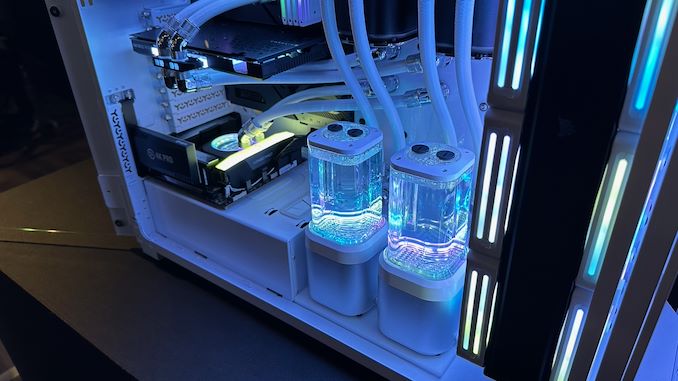
<p>Foveated rendering aside, XPG is making sure that the Nia won't be a one-trick pony. The handheld's other major claim to fame is its hardware swappability. The prototype handheld not only features a removable M.2-2230 SSD, but the company is also taking advantage of the recently-introduced LPCAMM2 memory module standard to introduce removable DRAM. Via a hatch in the back of the handheld, device owners would be able to swap out LPCAMM2 LPDDR5X modules for higher capacity versions. This would give the handheld an additional degree of future-proofness over current handhelds, which use non-replaceable soldered-down memory.</p>
<p>Rounding out the package, the current prototype is based on an AMD's Zen 4 Phoenix APU, which is used across both of the company's current mobile lines (Ryzen Mobile 7000/8000 and Ryzen Z1). Meanwhile, the unit's display is adjustable, allowing it to be angled away from the body of the handheld.</p>
<p align="center"><a href="https://www.anandtech.com/show/21432/xpg-demos-nia-handheld-gaming-pc-foveated-rendering-swappable-dram"><img alt="" src="https://images.anandtech.com/doci/21432/IMG_9818-678-specs_575px.jpg" /></a></p>
<p>Assuming all goes well with the prototype, XPG aims to release a finished product in 2025.</p>
<p style="text-align: center;"><a href="https://www.anandtech.com/show/21432/xpg-demos-nia-handheld-gaming-pc-foveated-rendering-swappable-dram"><img alt="" src="https://images.anandtech.com/doci/21432/IMG_9824_575px.jpg" /></a></p>
</p> ADATA)
 and augmented reality (AR) applications by taking advantage of how human vision works. Typically, humans can only perceive detailed imagery in the relatively small central area of our vision called the fovea, while our peripheral vision is much less detailed. Dynamic foveated rendering, in turn, exploits this by using real-time eye tracking to determine where the user is looking, and then rendering just that area in high/full resolution, while rendering the peripheral areas in lower resolution. The net result is that only a fraction of the screen is rendered at full detail, which cuts down on the total amount of rendering work required and boosting framerates on performance-limited devices.</p>
<p style="text-align: center;"><a href="https://www.anandtech.com/show/21432/xpg-demos-nia-handheld-gaming-pc-foveated-rendering-swappable-dram"><img alt="" src="https://images.anandtech.com/doci/21432/IMG_9819_575px.jpg" /></a></p>
<p>As stated before, this technology is sometimes used in high-end AR/VR headsets, where high resolution displays are placed mere inches from one's face. This ends up being an ideal use case for the technique, since at those distances, only a small fraction of the screen is within the fovea.</p>
<p>Using dynamic foveated rendering for a handheld, on the other hand, is a more novel application. All of the same visual principles apply, but the resolutions at play are lower, and the screen is farther from the users' eyes. This makes a handheld device a less ideal use case, at least on paper, as a larger portion of the screen is going to be in the fovea, and thus will need to be rendered at full resolution. None the less, it will be interesting to see how XPG's efforts pan out, and if dynamic foveated rendering is beneficial enough for handheld PCs. As we sometimes see with trade show demos, not everything makes it out of the prototype stage.</p>
<p align="center"><a href="https://www.anandtech.com/show/21432/xpg-demos-nia-handheld-gaming-pc-foveated-rendering-swappable-dram"><img alt="" src="https://images.anandtech.com/doci/21432/IMG_9823_575px.jpg" /></a></p>
<p>According to a press release put out by ADATA ahead of the trade show, the eye tracking technology is being provided by AMD collaborator <a href="https://beam.eyeware.tech/">Eyeware</a>. Notably, their software-based approach runs on top of standard webcams, rather than requiring IR cameras. So the camera hardware itself should be pretty straight-forward.</p>
<p>Foveated rendering aside, XPG is making sure that the Nia won't be a one-trick pony. The handheld's other major claim to fame is its hardware swappability. The prototype handheld not only features a removable M.2-2230 SSD, but the company is also taking advantage of the recently-introduced LPCAMM2 memory module standard to introduce removable DRAM. Via a hatch in the back of the handheld, device owners would be able to swap out LPCAMM2 LPDDR5X modules for higher capacity versions. This would give the handheld an additional degree of future-proofness over current handhelds, which use non-replaceable soldered-down memory.</p>
<p>Rounding out the package, the current prototype is based on an AMD's Zen 4 Phoenix APU, which is used across both of the company's current mobile lines (Ryzen Mobile 7000/8000 and Ryzen Z1). Meanwhile, the unit's display is adjustable, allowing it to be angled away from the body of the handheld.</p>
<p align="center"><a href="https://www.anandtech.com/show/21432/xpg-demos-nia-handheld-gaming-pc-foveated-rendering-swappable-dram"><img alt="" src="https://images.anandtech.com/doci/21432/IMG_9818-678-specs_575px.jpg" /></a></p>
<p>Assuming all goes well with the prototype, XPG aims to release a finished product in 2025.</p>
<p style="text-align: center;"><a href="https://www.anandtech.com/show/21432/xpg-demos-nia-handheld-gaming-pc-foveated-rendering-swappable-dram"><img alt="" src="https://images.anandtech.com/doci/21432/IMG_9824_575px.jpg" /></a></p>
</p> ADATA | https://compbuddey.blogspot.com/2024/06/xpg-demos-nia-handheld-gaming-pc-with_23.html)
 and augmented reality (AR) applications by taking advantage of how human vision works. Typically, humans can only perceive detailed imagery in the relatively small central area of our vision called the fovea, while our peripheral vision is much less detailed. Dynamic foveated rendering, in turn, exploits this by using real-time eye tracking to determine where the user is looking, and then rendering just that area in high/full resolution, while rendering the peripheral areas in lower resolution. The net result is that only a fraction of the screen is rendered at full detail, which cuts down on the total amount of rendering work required and boosting framerates on performance-limited devices.</p>
<p style="text-align: center;"><a href="https://www.anandtech.com/show/21432/xpg-demos-nia-handheld-gaming-pc-foveated-rendering-swappable-dram"><img alt="" src="https://images.anandtech.com/doci/21432/IMG_9819_575px.jpg" /></a></p>
<p>As stated before, this technology is sometimes used in high-end AR/VR headsets, where high resolution displays are placed mere inches from one's face. This ends up being an ideal use case for the technique, since at those distances, only a small fraction of the screen is within the fovea.</p>
<p>Using dynamic foveated rendering for a handheld, on the other hand, is a more novel application. All of the same visual principles apply, but the resolutions at play are lower, and the screen is farther from the users' eyes. This makes a handheld device a less ideal use case, at least on paper, as a larger portion of the screen is going to be in the fovea, and thus will need to be rendered at full resolution. None the less, it will be interesting to see how XPG's efforts pan out, and if dynamic foveated rendering is beneficial enough for handheld PCs. As we sometimes see with trade show demos, not everything makes it out of the prototype stage.</p>
<p align="center"><a href="https://www.anandtech.com/show/21432/xpg-demos-nia-handheld-gaming-pc-foveated-rendering-swappable-dram"><img alt="" src="https://images.anandtech.com/doci/21432/IMG_9823_575px.jpg" /></a></p>
<p>According to a press release put out by ADATA ahead of the trade show, the eye tracking technology is being provided by AMD collaborator <a href="https://beam.eyeware.tech/">Eyeware</a>. Notably, their software-based approach runs on top of standard webcams, rather than requiring IR cameras. So the camera hardware itself should be pretty straight-forward.</p>
<p>Foveated rendering aside, XPG is making sure that the Nia won't be a one-trick pony. The handheld's other major claim to fame is its hardware swappability. The prototype handheld not only features a removable M.2-2230 SSD, but the company is also taking advantage of the recently-introduced LPCAMM2 memory module standard to introduce removable DRAM. Via a hatch in the back of the handheld, device owners would be able to swap out LPCAMM2 LPDDR5X modules for higher capacity versions. This would give the handheld an additional degree of future-proofness over current handhelds, which use non-replaceable soldered-down memory.</p>
<p>Rounding out the package, the current prototype is based on an AMD's Zen 4 Phoenix APU, which is used across both of the company's current mobile lines (Ryzen Mobile 7000/8000 and Ryzen Z1). Meanwhile, the unit's display is adjustable, allowing it to be angled away from the body of the handheld.</p>
<p align="center"><a href="https://www.anandtech.com/show/21432/xpg-demos-nia-handheld-gaming-pc-foveated-rendering-swappable-dram"><img alt="" src="https://images.anandtech.com/doci/21432/IMG_9818-678-specs_575px.jpg" /></a></p>
<p>Assuming all goes well with the prototype, XPG aims to release a finished product in 2025.</p>
<p style="text-align: center;"><a href="https://www.anandtech.com/show/21432/xpg-demos-nia-handheld-gaming-pc-foveated-rendering-swappable-dram"><img alt="" src="https://images.anandtech.com/doci/21432/IMG_9824_575px.jpg" /></a></p>
</p> ADATA&body=https://compbuddey.blogspot.com/2024/06/xpg-demos-nia-handheld-gaming-pc-with_23.html)
0 Comments