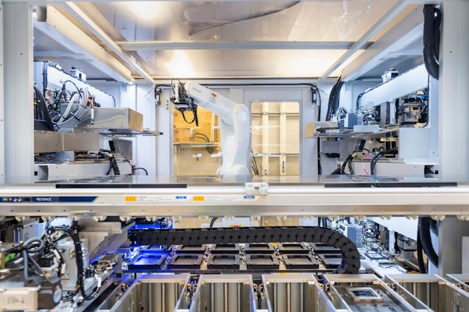

To say that the global foundry market is booming right now would be an understatement. Demand for leading-edge process technologies driven by AI and HPC applications is unprecedented, and with Intel joining the contract chipmaking game, this market segment is once again becoming rather competitive as well. Yet, this is exactly the market segment that Rapidus, a foundry startup backed by the Japanese government and several major Japanese companies, is going to enter in 2027, when its first fab comes online, just a few years from now.
In a fresh update on the status of bringing up the company's first leading-edge fab, Rapidus has revealed that they are intending to get in to the chip packaging game as well. Once complete, the ¥5 trillion ($32 billion) fab will be offering both chip lithography on a 2nm node, as well as packaging services for chips produced within the facility – a notable distinction in an industry where, even if packaging isn't outsourced entirely (OSAT), it's still normally handled at dedicated facilities.
Ultimately, while the company wants to serve the same clients as TSMC, Samsung, and Intel Foundry, the firm plans to do things almost completely differently than its competitors in a bid to speed up chipmaking from finishing design to getting a working chip out of the fab.
"We are very proud of being Japanese," said Henri Richard, general manager and president of Rapidus's subsidiary in the U.S. "[…] I know that some people may be looking at this thinking [that] Japan is known for quality, attention to detail, but not necessarily for speed, or flexibility. But I will tell you that Atsuyoshi Koike (the head of Rapidus) is a very special executive. That is, he has all the quality of Japan, with a lot of American thinking. So he is quite a unique guy, and certainly extraordinarily focused on creating a company that will be extremely flexible and extremely quick on its feet."
Perhaps the most significant difference between Rapidus and traditional foundries is that the company will offer only leading-edge manufacturing technologies to its clients: 2 nm in 2027 (phase 1) and then 1.4 nm in the future (phase 2). This is a stark contrast with other contract fabs, including Intel, which tend to offer their customers a full range of fabrication processes to land more clients and produce more chips. Apparently, Rapidus hopes that that there will be enough Japanese and American chip developers that are inclined to use its 2 nm fabrication process to produce their designs. With that said, the number of chip designers that are using the most advanced production node at any given time is relatively small – limited to large firms who need first-mover advantage and have the margins to justify taking the risk – so it remains to be seen whether Rapidus's business model becomes successful. The company believes it will, since the market of chips made on advanced nodes is growing rapidly.
"Until recently IDC was giving a an estimation of the 2nm and below market as about $80 billion and I think we are going to see soon a revision of the potential to $150 billion," said Richard. "[…] TSMC is the 800 pound gorilla in the space. Samsung is there and Intel is going to enter that space. But the market growth is so significant and the demand is so high, that it does not take a lot of market share for Rapidus to be successful. One of the things that gives me great comfort is that when I talk to our EDA partners, when I talk to our potential clients, it is obvious that the entire industry is looking for alternative supply from a fully independent foundry. There is a place for Samsung in this industry, there is a place for Intel in this industry, the industry is currently owned by TSMC. But another totally independent foundry is more than welcome by all of the ecosystem partners and by the customers. So, I feel really, really good about Rapidus's positioning."
Speaking of advanced process technologies, it is notable that Rapidus does not plan to use ASML's High-NA Twinscan EXE lithography scanners for 2 nm production. Instead, Rapidus is sticking to ASML's proven Low-NA scanners, which will reduce costs of Rapidus's fab, though it will entail usage of EUV double patterning, which brings up costs and lengthens the production cycle in other ways. Even with those trade-offs, SemiAnalysis analysts believe that given the cost of High-NA EUV litho tools and halved imaging field, ... Semiconductors


A few years back, the Japanese government's New Energy and Industrial Technology Development Organization (NEDO ) allocated funding for the development of green datacenter technologies. With the aim to obtain up to 40% savings in overall power consumption, several Japanese companies have been developing an optical interface for their enterprise SSDs. And at this year's FMS, Kioxia had their optical interface on display.

For this demonstration, Kioxia took its existing CM7 enterprise SSD and created an optical interface for it. A PCIe card with on-board optics developed by Kyocera is installed in the server slot. An optical interface allows data transfer over long distances (it was 40m in the demo, but Kioxia promises lengths of up to 100m for the cable in the future). This allows the storage to be kept in a separate room with minimal cooling requirements compared to the rack with the CPUs and GPUs. Disaggregation of different server components will become an option as very high throughput interfaces such as PCIe 7.0 (with 128 GT/s rates) become available.

The demonstration of the optical SSD showed a slight loss in IOPS performance, but a significant advantage in the latency metric over the shipping enterprise SSD behind a copper network link. Obviously, there are advantages in wiring requirements and signal integrity maintenance with optical links.
Being a proof-of-concept demonstration, we do see the requirement for an industry-standard approach if this were to gain adoption among different datacenter vendors. The PCI-SIG optical workgroup will need to get its act together soon to create a standards-based approach to this problem.
Storage

Under the CHIPS & Science Act, the U.S. government provided tens of billions of dollars in grants and loans to the world's leading maker of chips, such as Intel, Samsung, and TSMC, which will significantly expand the country's semiconductor production industry in the coming years. However, most chips are typically tested, assembled, and packaged in Asia, which has left the American supply chain incomplete. Addressing this last gap in the government's domestic chip production plans, these past couple of weeks the U.S. government signed memorandums of understanding worth about $1.5 billion with Amkor and SK hynix to support their efforts to build chip packaging facilities in the U.S.
Amkor plans to build a $2 billion advanced packaging facility near Peoria, Arizona, to test and assemble chips produced by TSMC at its Fab 21 near Phoenix, Arizona. The company signed a MOU that offers $400 million in direct funding and access to $200 million in loans under the CHIPS & Science Act. In addition, the company plans to take advantage of a 25% investment tax credit on eligible capital expenditures.
Set to be strategically positioned near TSMC's upcoming Fab 21 complex in Arizona, Amkor's Peoria facility will occupy 55 acres and, when fully completed, will feature over 500,000 square feet (46,451 square meters) of cleanroom space, more than twice the size of Amkor's advanced packaging site in Vietnam. Although the company has not disclosed the exact capacity or the specific technologies the facility will support, it is expected to cater to a wide range of industries, including automotive, high-performance computing, and mobile technologies. This suggests the new plant will offer diverse packaging solutions, including traditional, 2.5D, and 3D technologies.
Amkor has collaborated extensively with Apple on the vision and initial setup of the Peoria facility, as Apple is slated to be the facility's first and largest customer, marking a significant commitment from the tech giant. This partnership highlights the importance of the new facility in reinforcing the U.S. semiconductor supply chain and positioning Amkor as a key partner for companies relying on TSMC's manufacturing capabilities. The project is expected to generate around 2,000 jobs and is scheduled to begin operations in 2027.
This week SK hynix also signed a preliminary agreement with the U.S. government to receive up to $450 million in direct funding and $500 million in loans to build an advanced memory packaging facility in West Lafayette, Indiana.
The proposed facility is scheduled to begin operations in 2028, which means that it will assemble HBM4 or HBM4E memory. Meanwhile, DRAM devices for high bandwidth memory (HBM) stacks will still be produced in South Korea. Nonetheless, packing finished HBM4/HBM4E in the U.S. and possibly integrating these memory modules with high-end processors is a big deal.
In addition to building its packaging plant, SK hynix plans to collaborate with Purdue University and other local research institutions to advance semiconductor technology and packaging innovations. This partnership is intended to bolster research and development in the region, positioning the facility as a hub for AI technology and skilled employment.
Semiconductors

Kioxia's booth at FMS 2024 was a busy one with multiple technology demonstrations keeping visitors occupied. A walk-through of the BiCS 8 manufacturing process was the first to grab my attention. Kioxia and Western Digital announced the sampling of BiCS 8 in March 2023. We had touched briefly upon its CMOS Bonded Array (CBA) scheme in our coverage of Kioxial's 2Tb QLC NAND device and coverage of Western Digital's 128 TB QLC enterprise SSD proof-of-concept demonstration. At Kioxia's booth, we got more insights.

Traditionally, fabrication of flash chips involved placement of the associate logic circuitry (CMOS process) around the periphery of the flash array. The process then moved on to putting the CMOS under the cell array, but the wafer development process was serialized with the CMOS logic getting fabricated first followed by the cell array on top. However, this has some challenges because the cell array requires a high-temperature processing step to ensure higher reliability that can be detrimental to the health of the CMOS logic. Thanks to recent advancements in wafer bonding techniques, the new CBA process allows the CMOS wafer and cell array wafer to be processed independently in parallel and then pieced together, as shown in the models above.

The BiCS 8 3D NAND incorporates 218 layers, compared to 112 layers in BiCS 5 and 162 layers in BiCS 6. The company decided to skip over BiCS 7 (or, rather, it was probably a short-lived generation meant as an internal test vehicle). The generation retains the four-plane charge trap structure of BiCS 6. In its TLC avatar, it is available as a 1 Tbit device. The QLC version is available in two capacities - 1 Tbit and 2 Tbit.
Kioxia also noted that while the number of layers (218) doesn't compare favorably with the latest layer counts from the competition, its lateral scaling / cell shrinkage has enabled it to be competitive in terms of bit density as well as operating speeds (3200 MT/s). For reference, the latest shipping NAND from Micron - the G9 - has 276 layers with a bit density in TLC mode of 21 Gbit/mm2, and operates at up to 3600 MT/s. However, its 232L NAND operates only up to 2400 MT/s and has a bit density of 14.6 Gbit/mm2.
It must be noted that the CBA hybrid bonding process has advantages over the current processes used by other vendors - including Micron's CMOS under array (CuA) and SK hynix's 4D PUC (periphery-under-chip) developed in the late 2010s. It is expected that other NAND vendors will also move eventually to some variant of the hybrid bonding scheme used by Kioxia.
Storage
Lorem Ipsum is simply dummy text of the printing and typesetting industry. Lorem Ipsum has been the industry's.


 fab will be offering both chip lithography on a 2nm node, as well as packaging services for chips produced within the facility – a notable distinction in an industry where, even if packaging isn't outsourced entirely (OSAT), it's still normally handled at dedicated facilities.</p>
<p>Ultimately, while the company wants to serve the same clients as TSMC, Samsung, and Intel Foundry, the firm plans to do things almost completely differently than its competitors in a bid to speed up chipmaking from finishing design to getting a working chip out of the fab.</p>
<p>"We are very proud of being Japanese," said Henri Richard, general manager and president of Rapidus's subsidiary in the U.S. "[…] I know that some people may be looking at this thinking [that] Japan is known for quality, attention to detail, but not necessarily for speed, or flexibility. But I will tell you that Atsuyoshi Koike (the head of Rapidus) is a very special executive. That is, he has all the quality of Japan, with a lot of American thinking. So he is quite a unique guy, and certainly extraordinarily focused on creating a company that will be extremely flexible and extremely quick on its feet."</p>
<h3>2nm Only, At First</h3>
<p>Perhaps the most significant difference between Rapidus and traditional foundries is that the company will offer only leading-edge manufacturing technologies to its clients: 2 nm in 2027 (phase 1) and then 1.4 nm in the future (phase 2). This is a stark contrast with other contract fabs, including Intel, which tend to offer their customers a full range of fabrication processes to land more clients and produce more chips. Apparently, Rapidus hopes that that there will be enough Japanese and American chip developers that are inclined to use its 2 nm fabrication process to produce their designs. With that said, the number of chip designers that are using the most advanced production node at any given time is relatively small – limited to large firms who need first-mover advantage and have the margins to justify taking the risk – so it remains to be seen whether Rapidus's business model becomes successful. The company believes it will, since the market of chips made on advanced nodes is growing rapidly.</p>
<p>"Until recently IDC was giving a an estimation of the 2nm and below market as about $80 billion and I think we are going to see soon a revision of the potential to $150 billion," said Richard. "[…] TSMC is the 800 pound gorilla in the space. Samsung is there and Intel is going to enter that space. But the market growth is so significant and the demand is so high, that it does not take a lot of market share for Rapidus to be successful. One of the things that gives me great comfort is that when I talk to our EDA partners, when I talk to our potential clients, it is obvious that the entire industry is looking for alternative supply from a fully independent foundry. There is a place for Samsung in this industry, there is a place for Intel in this industry, the industry is currently owned by TSMC. But another totally independent foundry is more than welcome by all of the ecosystem partners and by the customers. So, I feel really, really good about Rapidus's positioning."</p>
<p>Speaking of advanced process technologies, it is notable that Rapidus does not plan to use ASML's High-NA Twinscan EXE lithography scanners for 2 nm production. Instead, Rapidus is sticking to ASML's proven Low-NA scanners, which will reduce costs of Rapidus's fab, though it will entail usage of EUV double patterning, which brings up costs and lengthens the production cycle in other ways. Even with those trade-offs, <a href="https://www.semianalysis.com/p/asml-dilemma-high-na-euv-is-worse">SemiAnalysis analysts believe</a> that given the cost of High-NA EUV litho tools and halved imaging field, ... Semiconductors)
 fab will be offering both chip lithography on a 2nm node, as well as packaging services for chips produced within the facility – a notable distinction in an industry where, even if packaging isn't outsourced entirely (OSAT), it's still normally handled at dedicated facilities.</p>
<p>Ultimately, while the company wants to serve the same clients as TSMC, Samsung, and Intel Foundry, the firm plans to do things almost completely differently than its competitors in a bid to speed up chipmaking from finishing design to getting a working chip out of the fab.</p>
<p>"We are very proud of being Japanese," said Henri Richard, general manager and president of Rapidus's subsidiary in the U.S. "[…] I know that some people may be looking at this thinking [that] Japan is known for quality, attention to detail, but not necessarily for speed, or flexibility. But I will tell you that Atsuyoshi Koike (the head of Rapidus) is a very special executive. That is, he has all the quality of Japan, with a lot of American thinking. So he is quite a unique guy, and certainly extraordinarily focused on creating a company that will be extremely flexible and extremely quick on its feet."</p>
<h3>2nm Only, At First</h3>
<p>Perhaps the most significant difference between Rapidus and traditional foundries is that the company will offer only leading-edge manufacturing technologies to its clients: 2 nm in 2027 (phase 1) and then 1.4 nm in the future (phase 2). This is a stark contrast with other contract fabs, including Intel, which tend to offer their customers a full range of fabrication processes to land more clients and produce more chips. Apparently, Rapidus hopes that that there will be enough Japanese and American chip developers that are inclined to use its 2 nm fabrication process to produce their designs. With that said, the number of chip designers that are using the most advanced production node at any given time is relatively small – limited to large firms who need first-mover advantage and have the margins to justify taking the risk – so it remains to be seen whether Rapidus's business model becomes successful. The company believes it will, since the market of chips made on advanced nodes is growing rapidly.</p>
<p>"Until recently IDC was giving a an estimation of the 2nm and below market as about $80 billion and I think we are going to see soon a revision of the potential to $150 billion," said Richard. "[…] TSMC is the 800 pound gorilla in the space. Samsung is there and Intel is going to enter that space. But the market growth is so significant and the demand is so high, that it does not take a lot of market share for Rapidus to be successful. One of the things that gives me great comfort is that when I talk to our EDA partners, when I talk to our potential clients, it is obvious that the entire industry is looking for alternative supply from a fully independent foundry. There is a place for Samsung in this industry, there is a place for Intel in this industry, the industry is currently owned by TSMC. But another totally independent foundry is more than welcome by all of the ecosystem partners and by the customers. So, I feel really, really good about Rapidus's positioning."</p>
<p>Speaking of advanced process technologies, it is notable that Rapidus does not plan to use ASML's High-NA Twinscan EXE lithography scanners for 2 nm production. Instead, Rapidus is sticking to ASML's proven Low-NA scanners, which will reduce costs of Rapidus's fab, though it will entail usage of EUV double patterning, which brings up costs and lengthens the production cycle in other ways. Even with those trade-offs, <a href="https://www.semianalysis.com/p/asml-dilemma-high-na-euv-is-worse">SemiAnalysis analysts believe</a> that given the cost of High-NA EUV litho tools and halved imaging field, ... Semiconductors | https://compbuddey.blogspot.com/2024/06/rapidus-adds-chip-packaging-services-to_11.html)
 fab will be offering both chip lithography on a 2nm node, as well as packaging services for chips produced within the facility – a notable distinction in an industry where, even if packaging isn't outsourced entirely (OSAT), it's still normally handled at dedicated facilities.</p>
<p>Ultimately, while the company wants to serve the same clients as TSMC, Samsung, and Intel Foundry, the firm plans to do things almost completely differently than its competitors in a bid to speed up chipmaking from finishing design to getting a working chip out of the fab.</p>
<p>"We are very proud of being Japanese," said Henri Richard, general manager and president of Rapidus's subsidiary in the U.S. "[…] I know that some people may be looking at this thinking [that] Japan is known for quality, attention to detail, but not necessarily for speed, or flexibility. But I will tell you that Atsuyoshi Koike (the head of Rapidus) is a very special executive. That is, he has all the quality of Japan, with a lot of American thinking. So he is quite a unique guy, and certainly extraordinarily focused on creating a company that will be extremely flexible and extremely quick on its feet."</p>
<h3>2nm Only, At First</h3>
<p>Perhaps the most significant difference between Rapidus and traditional foundries is that the company will offer only leading-edge manufacturing technologies to its clients: 2 nm in 2027 (phase 1) and then 1.4 nm in the future (phase 2). This is a stark contrast with other contract fabs, including Intel, which tend to offer their customers a full range of fabrication processes to land more clients and produce more chips. Apparently, Rapidus hopes that that there will be enough Japanese and American chip developers that are inclined to use its 2 nm fabrication process to produce their designs. With that said, the number of chip designers that are using the most advanced production node at any given time is relatively small – limited to large firms who need first-mover advantage and have the margins to justify taking the risk – so it remains to be seen whether Rapidus's business model becomes successful. The company believes it will, since the market of chips made on advanced nodes is growing rapidly.</p>
<p>"Until recently IDC was giving a an estimation of the 2nm and below market as about $80 billion and I think we are going to see soon a revision of the potential to $150 billion," said Richard. "[…] TSMC is the 800 pound gorilla in the space. Samsung is there and Intel is going to enter that space. But the market growth is so significant and the demand is so high, that it does not take a lot of market share for Rapidus to be successful. One of the things that gives me great comfort is that when I talk to our EDA partners, when I talk to our potential clients, it is obvious that the entire industry is looking for alternative supply from a fully independent foundry. There is a place for Samsung in this industry, there is a place for Intel in this industry, the industry is currently owned by TSMC. But another totally independent foundry is more than welcome by all of the ecosystem partners and by the customers. So, I feel really, really good about Rapidus's positioning."</p>
<p>Speaking of advanced process technologies, it is notable that Rapidus does not plan to use ASML's High-NA Twinscan EXE lithography scanners for 2 nm production. Instead, Rapidus is sticking to ASML's proven Low-NA scanners, which will reduce costs of Rapidus's fab, though it will entail usage of EUV double patterning, which brings up costs and lengthens the production cycle in other ways. Even with those trade-offs, <a href="https://www.semianalysis.com/p/asml-dilemma-high-na-euv-is-worse">SemiAnalysis analysts believe</a> that given the cost of High-NA EUV litho tools and halved imaging field, ... Semiconductors&body=https://compbuddey.blogspot.com/2024/06/rapidus-adds-chip-packaging-services-to_11.html)
0 Comments