

When Micron announced plans to build two new fabs in the U.S. in 2022, the company vaguely said both would come online by the decade's end. Then, in 2023, it began to optimize its spending, which pushed production at these fabrication facilities. This week, the company outlined more precise timeframes for when its fabs in Idaho and New York will start operations: this will happen from calendar 2026 to calendar 2029.
"These fab construction investments are necessary to support supply growth for the latter half of this decade," a statement by Micron in its Q3 FY2024 financial results report reads. "This Idaho fab will not contribute to meaningful bit supply until fiscal 2027 and the New York construction capex is not expected to contribute to bit supply growth until fiscal 2028 or later. The timing of future [wafer fab equipment] spend in these fabs will be managed to align supply growth with expected demand growth."
Micron's fiscal year 2027 starts in September 2026, so the new fab near Boise, Idaho, is set to start operations between September 2026 and September 2027. The company's fiscal 2028 starts in September 2027, so the fab will likely begin operations in calendar 2028 or later, probably depending on the demand for DRAM memory in the coming years. That said, Micron's U.S. memory fabs will begin operations between late 2026 and 2029, which aligns with the company's original plans.
Construction of the fab in Idaho is well underway. In contrast, construction of the New York facility has yet to begin as the company is working on regulatory and permitting processes in the state.
Micron's capital expenditure (CaPex) plan for FY2024 is approximately $8.0 billion, with a decrease in year-over-year spending on wafer fabrication equipment (WFE). In Q4 FY2024, the company will spend around $3 billion on fab construction, new wafer fab tools, and various expansions/upgrades.
Looking ahead to FY2025, the company plans a substantial increase in capex, targeting a mid-30s percentage of revenue to support various technological and facility advancements. In particular, it expects its quarterly CapEx to average above the $3 billion level seen in the fourth quarter of FY2024, which means that it plans to spend about $12 billion in its fiscal 2025, which begins in late September.
Half or more of the total CapEx increase in FY2025 (i.e., over $2 billion) will be allocated to constructing new fabs in Idaho and New York. Meanwhile, the FY2025 CapEx will significantly rise to fund high-bandwidth memory (HBM) assembly and testing and the construction of fabrication and back-end facilities. This increase also includes investments in technology transitions to meet growing demand.
"Fab construction in Idaho is underway, and we are working diligently to complete the regulatory and permitting processes in New York," said Sanjay Mehrotra, chief executive officer of Micron, at the company's conference call with investors and financial analysts (via SeekingAlpha). "This additional leading-edge greenfield capacity, along with continued technology transition investments in our Asia facilities, is required to meet long-term demand in the second half of this decade and beyond. These investments support our objective to maintain our current bit share over time and to grow our memory bit supply in line with long-term industry bit demand."
Memory

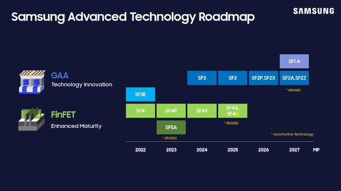
Samsung this week has unveiled its latest process technologies roadmap at the company's Samsung Foundry Forum (SFF) U.S. The new plan covers the evolution of Samsung's 2nm-class production nodes through 2027, including a process technology with a backside power delivery, re-emphasizing plans to bring out a 1.4nm-class node in 2027, and the introduction of a 'high value' 4nm-class manufacturing tech.
Samsung Foundry's key announcements for today are clearly focused on the its 2nm-class process technologies, which are set to enter production in 2025 and will span to 2027, when the company's 1.4-nm class production node is set to enter the scene. Samsung is also adding (or rather, renaming) another 2nm-class node to their roadmap with SF2, which was previously disclosed by Samsung as SF3P and aimed at high-performance devices.
"We have refined and improved the SF3P, resulting in what we now refer to as SF2," a Samsung spokesperson told AnandTech. "This enhanced node incorporates various process design improvements, delivering notable power, performance, and area (PPA) benefits."
| Samsung Foundry for Leading-Edge Nodes Announced on June 12, 2024 Compiled by AnandTech |
||||||||
| HVM Start | 2023 | 2024 | 2025 | 2026 | 2027 | 2027 | ||
| Process | SF3E | SF3 | SF2 (aka SF3P) |
SF2P/SF2X | SF2Z | SF1.4 | ||
| FET | GAAFET | |||||||
| Power Delivery | Frontside | Backside (BSPDN) | ? | |||||
| EUV | 0.33 NA EUV | ? | ? | ? | ? | |||
This is another example of a rebranding of leading-edge fabrication nodes in the recent years by a major chipmaker. Samsung Foundry is not disclosing any specific PPA improvements SF3P has over SF2, and for now is only stating in high-level terms that it will be a better-performing node than the planned SF3P.
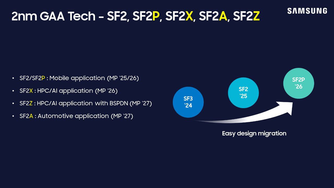
Meanwhile, this week's announcement also includes new information on Samsung's next batch of process nodes, which are planned for 2026 and 2027. In 2026 Samsung will have SF2P, a further refinement of SF2 which incorporates 'faster' yet less dense transistors. That will be followed up in 2027 with SF2Z, which adds backside power delivery to the mix for better and higher quality power delivery. In particular, Samsung is targetting voltate drop (aka IR drop) here, which is an ongoing concern in chip design.
Finally, SF1.4, a 1.4nm-class node, is on track for 2027 as well. Interestingly, however, it looks like it does not feature a backside power delivery. Which, per current roadmaps, would have Samsung as the only foundry not using BSPDN for their first 1.4nm/14Å-class node.
"We have optimized BSPDN and incorporated it for the first time in the SF2Z node we announced today," the spokesperso... Semiconductors

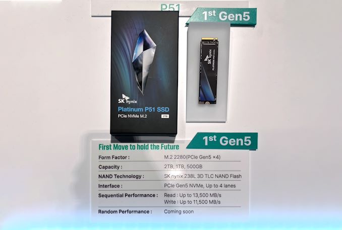
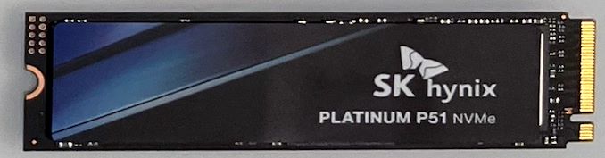
SK hynix is set to unveil their first Gen5 consumer NVMe SSD lineup shortly, based on the products at display in their GTC 2024 booth. The Platinum P51 M.2 2280 NVMe SSD will take over flagship duties from the Platinum P41 that has been serving the market for more than a year.
Similar to the Gold P31 and the Platinum P41, the Platinum P51 also uses an in-house SSD controller. The key updates are the move to PCIe Gen5 and the use of SK hynix's 238L TLC NAND. Other details are scarce, and we have reached out for additional information.
| SK hynix Platinum P51 Gen5 NVMe SSD Specifications | ||||
| Capacity | 500 GB | 1 TB | 2 TB | |
| Controller | SK hynix In-House (Alistar) | |||
| NAND Flash | SK hynix 238L 3D TLC NAND at ?? MT/s ('4D' with CMOS circuitry under the NAND as per SK hynix marketing) | |||
| Form-Factor, Interface | M.2-2280, PCIe 5.0 x4, NVMe 2.0 | |||
| Sequential Read | 13500 MB/s | |||
| Sequential Write | 11500 MB/s | |||
| Random Read IOPS | TBD | |||
| Random Write IOPS | TBD | |||
| SLC Caching | Yes | |||
| TCG Opal Encryption | TBD | |||
| Warranty | TBD | |||
| Write Endurance | TBD | TBD | TBD | |
Only the peak sequential access numbers were available at the GTC booth, indicating that the drive's firmware is still undergoing tweaks. It is also unclear how these numbers are going to vary based on capacity. Availability and pricing are also not public yet.
This is a significant launch for the Gen5 consumer SSD market, where the number of available options are quite limited. The Phison E26 controller and Micron's B58R NAND combination is already in its second generation (with the NAND operating at 2400 MT/s in the newest avatar), but other vertically integrated vendors such as Samsung, Western Digital / Kioxia, and SK hynix (till now) are focusing more on the Gen4 market which has much higher adoption.
We will update the piece with additional information once the specifications are officially available.
Storage
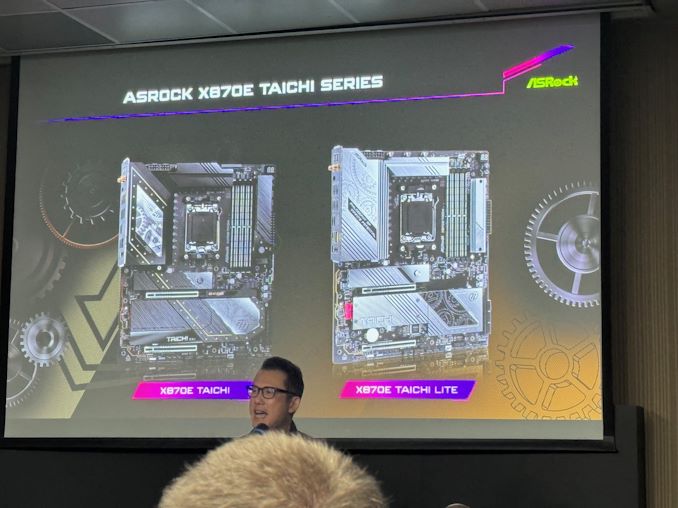
During Computex 2024, ASRock held an event to unveil some of its upcoming X870E motherboards, designed for AMD's Zen 5-based Ryzen 9000 series processors. ASRock's announcement includes a pair of Taichi-branded boards, the X870E Taichi and the lighter X870E Taichi lite, which uses AMD's X870E (Promontory 21) chipset for AM5.
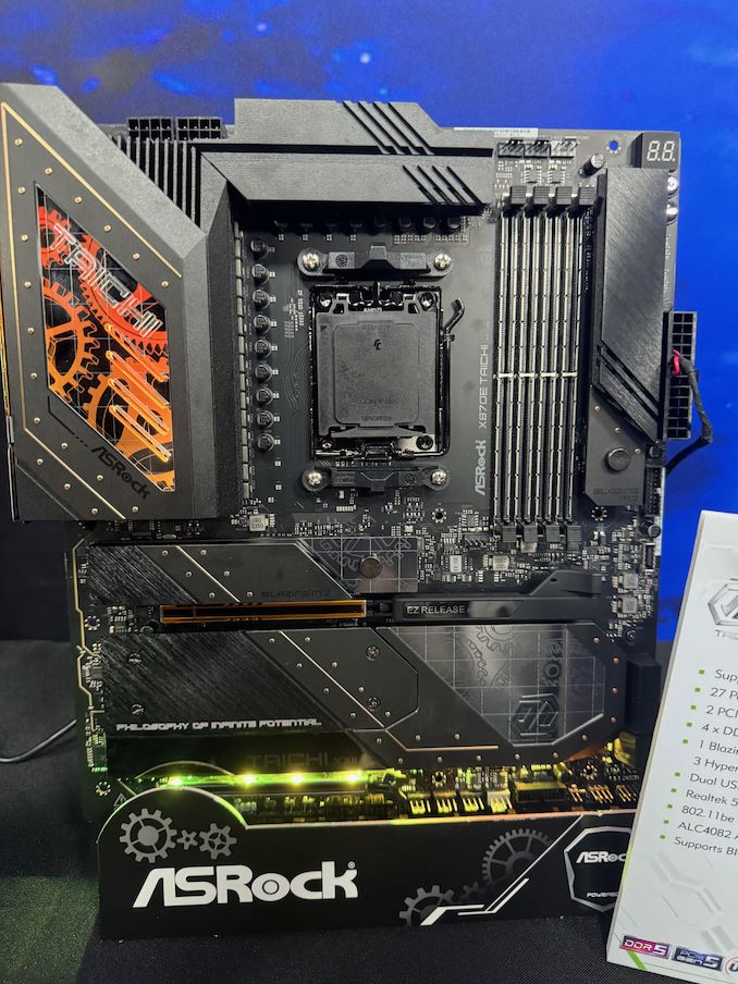
The current flagship model announced from ASRock's X870E line-up for Ryzen 9000 is the ASRock X870E Taichi. ASRock is advertising a large 27-phase power delivery through 110A SPS, suggesting this board is designed for overclockers and all-around power users. Two PCIe 5.0 x16 slots (operating in either x16/x0 or x8/x8) provide high-speed bandwidth for cutting-edge graphics cards and other devices. Meanwhile, ASRock has gone with 4 DIMM slots on this board, so system builders will be able to max out the board's memory capacity at the cost of bandwidth.
The storage offering is impressive; besides the obligatory PCIe Gen5 x4 M.2 slot (Blazing M.2), ASRock has outfit the board with another three PCIe Gen4 x4 (Hyper) M.2 slots. Also present are two USB4 Type-C ports for high-bandwidth external I/O, while networking support is a solid pairing of a discrete Wi-Fi 7 controller with a Realtek 5Gb Ethernet controller (and the first AM5 board we've come across with something faster than a 2.5GbE controller).
The audio setup includes a Realtek ALC4082 codec and ESS SABRE9218 DAC supporting high-fidelity sound. The BIOS flashback feature is also a nice touch, and we believe this should be a feature on all mid-range to high-end motherboards, which provides an easy way to update the firmware without installing a CPU. And, as no high-end board would be complete without it, ASRock has put RGB lighting on the X870E Taichi as well.
Ultimately, as ASRock's high-end X870E board, the X870E Taichi comes with pretty much every last cutting-edge technology that ASRock can fit on the board.
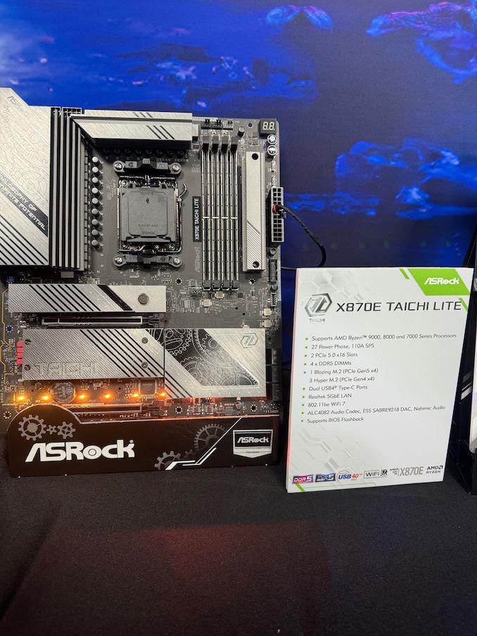
Comparatively, the ASRock X870E Taichi Lite is a more streamlined and functional version of the X870E Taichi. The Lite retaining all of the latter's key features, including the 27-phase power delivery with 110A smart power stages, dual PCIe 5.0 x16 slots operating at x16 or x8/x8, four DDR5 DIMM slots, and four M.2 slots (1x Gen5 + 3x Gen4). The only significant difference is aesthetics: the Taichi Lite features a simpler silver-themed design without the RGB lighting, while the standard Taichi has a more intricate gold-accented and fanciful aesthetics.
In terms of availability, ASRock is not disclosing a release date for the board at the show. And, checking around with other tech journalists, Andreas Schilling from HawrdwareLUXX has heard that X870E and X870 motherboards aren't expected to be available in time for the Ryzen 9000 series launch. We will investigate this and contact the motherboard vendors to confirm the situation. Though as X870E/X870 boards barely differ from the current crop of X670E/B650E boards to begin with, the Ryzen 9000 series won't be fazed by a lack of slightly newer motherboards.
Motherboards
Samsung this week has unveiled its latest process technologies roadmap at the company's Samsung Foundry Forum (SFF) U.S. The new plan covers the evolution of Samsung's 2nm-class production nodes through 2027, including a process technology with a backside power delivery, re-emphasizing plans to bring out a 1.4nm-class node in 2027, and the introduction of a 'high value' 4nm-class manufacturing tech.
Samsung Foundry's key announcements for today are clearly focused on the its 2nm-class process technologies, which are set to enter production in 2025 and will span to 2027, when the company's 1.4-nm class production node is set to enter the scene. Samsung is also adding (or rather, renaming) another 2nm-class node to their roadmap with SF2, which was previously disclosed by Samsung as SF3P and aimed at high-performance devices.
"We have refined and improved the SF3P, resulting in what we now refer to as SF2," a Samsung spokesperson told AnandTech. "This enhanced node incorporates various process design improvements, delivering notable power, performance, and area (PPA) benefits."
| Samsung Foundry for Leading-Edge Nodes Announced on June 12, 2024 Compiled by AnandTech |
||||||||
| HVM Start | 2023 | 2024 | 2025 | 2026 | 2027 | 2027 | ||
| Process | SF3E | SF3 | SF2 (aka SF3P) |
SF2P/SF2X | SF2Z | SF1.4 | ||
| FET | GAAFET | |||||||
| Power Delivery | Frontside | Backside (BSPDN) | ? | |||||
| EUV | 0.33 NA EUV | ? | ? | ? | ? | |||
This is another example of a rebranding of leading-edge fabrication nodes in the recent years by a major chipmaker. Samsung Foundry is not disclosing any specific PPA improvements SF3P has over SF2, and for now is only stating in high-level terms that it will be a better-performing node than the planned SF3P.
Meanwhile, this week's announcement also includes new information on Samsung's next batch of process nodes, which are planned for 2026 and 2027. In 2026 Samsung will have SF2P, a further refinement of SF2 which incorporates 'faster' yet less dense transistors. That will be followed up in 2027 with SF2Z, which adds backside power delivery to the mix for better and higher quality power delivery. In particular, Samsung is targetting voltate drop (aka IR drop) here, which is an ongoing concern in chip design.
Finally, SF1.4, a 1.4nm-class node, is on track for 2027 as well. Interestingly, however, it looks like it does not feature a backside power delivery. Which, per current roadmaps, would have Samsung as the only foundry not using BSPDN for their first 1.4nm/14Å-class node.
"We have optimized BSPDN and incorporated it for the first time in the SF2Z node we announced today," the spokesperso... Semiconductors
SK hynix is set to unveil their first Gen5 consumer NVMe SSD lineup shortly, based on the products at display in their GTC 2024 booth. The Platinum P51 M.2 2280 NVMe SSD will take over flagship duties from the Platinum P41 that has been serving the market for more than a year.
Similar to the Gold P31 and the Platinum P41, the Platinum P51 also uses an in-house SSD controller. The key updates are the move to PCIe Gen5 and the use of SK hynix's 238L TLC NAND. Other details are scarce, and we have reached out for additional information.
| SK hynix Platinum P51 Gen5 NVMe SSD Specifications | ||||
| Capacity | 500 GB | 1 TB | 2 TB | |
| Controller | SK hynix In-House (Alistar) | |||
| NAND Flash | SK hynix 238L 3D TLC NAND at ?? MT/s ('4D' with CMOS circuitry under the NAND as per SK hynix marketing) | |||
| Form-Factor, Interface | M.2-2280, PCIe 5.0 x4, NVMe 2.0 | |||
| Sequential Read | 13500 MB/s | |||
| Sequential Write | 11500 MB/s | |||
| Random Read IOPS | TBD | |||
| Random Write IOPS | TBD | |||
| SLC Caching | Yes | |||
| TCG Opal Encryption | TBD | |||
| Warranty | TBD | |||
| Write Endurance | TBD | TBD | TBD | |
Only the peak sequential access numbers were available at the GTC booth, indicating that the drive's firmware is still undergoing tweaks. It is also unclear how these numbers are going to vary based on capacity. Availability and pricing are also not public yet.
This is a significant launch for the Gen5 consumer SSD market, where the number of available options are quite limited. The Phison E26 controller and Micron's B58R NAND combination is already in its second generation (with the NAND operating at 2400 MT/s in the newest avatar), but other vertically integrated vendors such as Samsung, Western Digital / Kioxia, and SK hynix (till now) are focusing more on the Gen4 market which has much higher adoption.
We will update the piece with additional information once the specifications are officially available.
Storage
During Computex 2024, ASRock held an event to unveil some of its upcoming X870E motherboards, designed for AMD's Zen 5-based Ryzen 9000 series processors. ASRock's announcement includes a pair of Taichi-branded boards, the X870E Taichi and the lighter X870E Taichi lite, which uses AMD's X870E (Promontory 21) chipset for AM5.
The current flagship model announced from ASRock's X870E line-up for Ryzen 9000 is the ASRock X870E Taichi. ASRock is advertising a large 27-phase power delivery through 110A SPS, suggesting this board is designed for overclockers and all-around power users. Two PCIe 5.0 x16 slots (operating in either x16/x0 or x8/x8) provide high-speed bandwidth for cutting-edge graphics cards and other devices. Meanwhile, ASRock has gone with 4 DIMM slots on this board, so system builders will be able to max out the board's memory capacity at the cost of bandwidth.
The storage offering is impressive; besides the obligatory PCIe Gen5 x4 M.2 slot (Blazing M.2), ASRock has outfit the board with another three PCIe Gen4 x4 (Hyper) M.2 slots. Also present are two USB4 Type-C ports for high-bandwidth external I/O, while networking support is a solid pairing of a discrete Wi-Fi 7 controller with a Realtek 5Gb Ethernet controller (and the first AM5 board we've come across with something faster than a 2.5GbE controller).
The audio setup includes a Realtek ALC4082 codec and ESS SABRE9218 DAC supporting high-fidelity sound. The BIOS flashback feature is also a nice touch, and we believe this should be a feature on all mid-range to high-end motherboards, which provides an easy way to update the firmware without installing a CPU. And, as no high-end board would be complete without it, ASRock has put RGB lighting on the X870E Taichi as well.
Ultimately, as ASRock's high-end X870E board, the X870E Taichi comes with pretty much every last cutting-edge technology that ASRock can fit on the board.
Comparatively, the ASRock X870E Taichi Lite is a more streamlined and functional version of the X870E Taichi. The Lite retaining all of the latter's key features, including the 27-phase power delivery with 110A smart power stages, dual PCIe 5.0 x16 slots operating at x16 or x8/x8, four DDR5 DIMM slots, and four M.2 slots (1x Gen5 + 3x Gen4). The only significant difference is aesthetics: the Taichi Lite features a simpler silver-themed design without the RGB lighting, while the standard Taichi has a more intricate gold-accented and fanciful aesthetics.
In terms of availability, ASRock is not disclosing a release date for the board at the show. And, checking around with other tech journalists, Andreas Schilling from HawrdwareLUXX has heard that X870E and X870 motherboards aren't expected to be available in time for the Ryzen 9000 series launch. We will investigate this and contact the motherboard vendors to confirm the situation. Though as X870E/X870 boards barely differ from the current crop of X670E/B650E boards to begin with, the Ryzen 9000 series won't be fazed by a lack of slightly newer motherboards.
Motherboards
Lorem Ipsum is simply dummy text of the printing and typesetting industry. Lorem Ipsum has been the industry's.
Samsung this week has unveiled its latest process technologies roadmap at the company's Samsung Foundry Forum (SFF) U.S. The new plan covers the evolution of Samsung's 2nm-class production nodes through 2027, including a process technology with a backside power delivery, re-emphasizing plans to bring out a 1.4nm-class node in 2027, and the introduction of a 'high value' 4nm-class manufacturing tech.
Samsung Foundry's key announcements for today are clearly focused on the its 2nm-class process technologies, which are set to enter production in 2025 and will span to 2027, when the company's 1.4-nm class production node is set to enter the scene. Samsung is also adding (or rather, renaming) another 2nm-class node to their roadmap with SF2, which was previously disclosed by Samsung as SF3P and aimed at high-performance devices.
"We have refined and improved the SF3P, resulting in what we now refer to as SF2," a Samsung spokesperson told AnandTech. "This enhanced node incorporates various process design improvements, delivering notable power, performance, and area (PPA) benefits."
| Samsung Foundry for Leading-Edge Nodes Announced on June 12, 2024 Compiled by AnandTech |
||||||||
| HVM Start | 2023 | 2024 | 2025 | 2026 | 2027 | 2027 | ||
| Process | SF3E | SF3 | SF2 (aka SF3P) |
SF2P/SF2X | SF2Z | SF1.4 | ||
| FET | GAAFET | |||||||
| Power Delivery | Frontside | Backside (BSPDN) | ? | |||||
| EUV | 0.33 NA EUV | ? | ? | ? | ? | |||
This is another example of a rebranding of leading-edge fabrication nodes in the recent years by a major chipmaker. Samsung Foundry is not disclosing any specific PPA improvements SF3P has over SF2, and for now is only stating in high-level terms that it will be a better-performing node than the planned SF3P.
Meanwhile, this week's announcement also includes new information on Samsung's next batch of process nodes, which are planned for 2026 and 2027. In 2026 Samsung will have SF2P, a further refinement of SF2 which incorporates 'faster' yet less dense transistors. That will be followed up in 2027 with SF2Z, which adds backside power delivery to the mix for better and higher quality power delivery. In particular, Samsung is targetting voltate drop (aka IR drop) here, which is an ongoing concern in chip design.
Finally, SF1.4, a 1.4nm-class node, is on track for 2027 as well. Interestingly, however, it looks like it does not feature a backside power delivery. Which, per current roadmaps, would have Samsung as the only foundry not using BSPDN for their first 1.4nm/14Å-class node.
"We have optimized BSPDN and incorporated it for the first time in the SF2Z node we announced today," the spokesperso... Semiconductors
SK hynix is set to unveil their first Gen5 consumer NVMe SSD lineup shortly, based on the products at display in their GTC 2024 booth. The Platinum P51 M.2 2280 NVMe SSD will take over flagship duties from the Platinum P41 that has been serving the market for more than a year.
Similar to the Gold P31 and the Platinum P41, the Platinum P51 also uses an in-house SSD controller. The key updates are the move to PCIe Gen5 and the use of SK hynix's 238L TLC NAND. Other details are scarce, and we have reached out for additional information.
| SK hynix Platinum P51 Gen5 NVMe SSD Specifications | ||||
| Capacity | 500 GB | 1 TB | 2 TB | |
| Controller | SK hynix In-House (Alistar) | |||
| NAND Flash | SK hynix 238L 3D TLC NAND at ?? MT/s ('4D' with CMOS circuitry under the NAND as per SK hynix marketing) | |||
| Form-Factor, Interface | M.2-2280, PCIe 5.0 x4, NVMe 2.0 | |||
| Sequential Read | 13500 MB/s | |||
| Sequential Write | 11500 MB/s | |||
| Random Read IOPS | TBD | |||
| Random Write IOPS | TBD | |||
| SLC Caching | Yes | |||
| TCG Opal Encryption | TBD | |||
| Warranty | TBD | |||
| Write Endurance | TBD | TBD | TBD | |
Only the peak sequential access numbers were available at the GTC booth, indicating that the drive's firmware is still undergoing tweaks. It is also unclear how these numbers are going to vary based on capacity. Availability and pricing are also not public yet.
This is a significant launch for the Gen5 consumer SSD market, where the number of available options are quite limited. The Phison E26 controller and Micron's B58R NAND combination is already in its second generation (with the NAND operating at 2400 MT/s in the newest avatar), but other vertically integrated vendors such as Samsung, Western Digital / Kioxia, and SK hynix (till now) are focusing more on the Gen4 market which has much higher adoption.
We will update the piece with additional information once the specifications are officially available.
Storage
During Computex 2024, ASRock held an event to unveil some of its upcoming X870E motherboards, designed for AMD's Zen 5-based Ryzen 9000 series processors. ASRock's announcement includes a pair of Taichi-branded boards, the X870E Taichi and the lighter X870E Taichi lite, which uses AMD's X870E (Promontory 21) chipset for AM5.
The current flagship model announced from ASRock's X870E line-up for Ryzen 9000 is the ASRock X870E Taichi. ASRock is advertising a large 27-phase power delivery through 110A SPS, suggesting this board is designed for overclockers and all-around power users. Two PCIe 5.0 x16 slots (operating in either x16/x0 or x8/x8) provide high-speed bandwidth for cutting-edge graphics cards and other devices. Meanwhile, ASRock has gone with 4 DIMM slots on this board, so system builders will be able to max out the board's memory capacity at the cost of bandwidth.
The storage offering is impressive; besides the obligatory PCIe Gen5 x4 M.2 slot (Blazing M.2), ASRock has outfit the board with another three PCIe Gen4 x4 (Hyper) M.2 slots. Also present are two USB4 Type-C ports for high-bandwidth external I/O, while networking support is a solid pairing of a discrete Wi-Fi 7 controller with a Realtek 5Gb Ethernet controller (and the first AM5 board we've come across with something faster than a 2.5GbE controller).
The audio setup includes a Realtek ALC4082 codec and ESS SABRE9218 DAC supporting high-fidelity sound. The BIOS flashback feature is also a nice touch, and we believe this should be a feature on all mid-range to high-end motherboards, which provides an easy way to update the firmware without installing a CPU. And, as no high-end board would be complete without it, ASRock has put RGB lighting on the X870E Taichi as well.
Ultimately, as ASRock's high-end X870E board, the X870E Taichi comes with pretty much every last cutting-edge technology that ASRock can fit on the board.
Comparatively, the ASRock X870E Taichi Lite is a more streamlined and functional version of the X870E Taichi. The Lite retaining all of the latter's key features, including the 27-phase power delivery with 110A smart power stages, dual PCIe 5.0 x16 slots operating at x16 or x8/x8, four DDR5 DIMM slots, and four M.2 slots (1x Gen5 + 3x Gen4). The only significant difference is aesthetics: the Taichi Lite features a simpler silver-themed design without the RGB lighting, while the standard Taichi has a more intricate gold-accented and fanciful aesthetics.
In terms of availability, ASRock is not disclosing a release date for the board at the show. And, checking around with other tech journalists, Andreas Schilling from HawrdwareLUXX has heard that X870E and X870 motherboards aren't expected to be available in time for the Ryzen 9000 series launch. We will investigate this and contact the motherboard vendors to confirm the situation. Though as X870E/X870 boards barely differ from the current crop of X670E/B650E boards to begin with, the Ryzen 9000 series won't be fazed by a lack of slightly newer motherboards.
Motherboards

 plan for FY2024 is approximately $8.0 billion, with a decrease in year-over-year spending on wafer fabrication equipment (WFE). In Q4 FY2024, the company will spend around $3 billion on fab construction, new wafer fab tools, and various expansions/upgrades.</p>
<p>Looking ahead to FY2025, the company plans a substantial increase in capex, targeting a mid-30s percentage of revenue to support various technological and facility advancements. In particular, it expects its quarterly CapEx to average above the $3 billion level seen in the fourth quarter of FY2024, which means that it plans to spend about $12 billion in its fiscal 2025, which begins in late September.</p>
<p>Half or more of the total CapEx increase in FY2025 (i.e., over $2 billion) will be allocated to constructing new fabs in Idaho and New York. Meanwhile, the FY2025 CapEx will significantly rise to fund high-bandwidth memory (HBM) assembly and testing and the construction of fabrication and back-end facilities. This increase also includes investments in technology transitions to meet growing demand. </p>
<p>"<em>Fab construction in Idaho is underway, and we are working diligently to complete the regulatory and permitting processes in New York,</em>" said Sanjay Mehrotra, chief executive officer of Micron, at the company's conference call with investors and financial analysts (via <a href="https://seekingalpha.com/article/4701253-micron-technology-inc-mu-q3-2024-earnings-call-transcript?source=content_type%3Areact%7Csection%3ATranscripts%7Csection_asset%3ATranscripts%7Cfirst_level_url%3Asymbol%7Cbutton%3ATitle%7Clock_status%3ANo%7Cline%3A1">SeekingAlpha</a>). "<em>This additional leading-edge greenfield capacity, along with continued technology transition investments in our Asia facilities, is required to meet long-term demand in the second half of this decade and beyond. These investments support our objective to maintain our current bit share over time and to grow our memory bit supply in line with long-term industry bit demand.</em>"</p>
</p> Memory)
 plan for FY2024 is approximately $8.0 billion, with a decrease in year-over-year spending on wafer fabrication equipment (WFE). In Q4 FY2024, the company will spend around $3 billion on fab construction, new wafer fab tools, and various expansions/upgrades.</p>
<p>Looking ahead to FY2025, the company plans a substantial increase in capex, targeting a mid-30s percentage of revenue to support various technological and facility advancements. In particular, it expects its quarterly CapEx to average above the $3 billion level seen in the fourth quarter of FY2024, which means that it plans to spend about $12 billion in its fiscal 2025, which begins in late September.</p>
<p>Half or more of the total CapEx increase in FY2025 (i.e., over $2 billion) will be allocated to constructing new fabs in Idaho and New York. Meanwhile, the FY2025 CapEx will significantly rise to fund high-bandwidth memory (HBM) assembly and testing and the construction of fabrication and back-end facilities. This increase also includes investments in technology transitions to meet growing demand. </p>
<p>"<em>Fab construction in Idaho is underway, and we are working diligently to complete the regulatory and permitting processes in New York,</em>" said Sanjay Mehrotra, chief executive officer of Micron, at the company's conference call with investors and financial analysts (via <a href="https://seekingalpha.com/article/4701253-micron-technology-inc-mu-q3-2024-earnings-call-transcript?source=content_type%3Areact%7Csection%3ATranscripts%7Csection_asset%3ATranscripts%7Cfirst_level_url%3Asymbol%7Cbutton%3ATitle%7Clock_status%3ANo%7Cline%3A1">SeekingAlpha</a>). "<em>This additional leading-edge greenfield capacity, along with continued technology transition investments in our Asia facilities, is required to meet long-term demand in the second half of this decade and beyond. These investments support our objective to maintain our current bit share over time and to grow our memory bit supply in line with long-term industry bit demand.</em>"</p>
</p> Memory)
 plan for FY2024 is approximately $8.0 billion, with a decrease in year-over-year spending on wafer fabrication equipment (WFE). In Q4 FY2024, the company will spend around $3 billion on fab construction, new wafer fab tools, and various expansions/upgrades.</p>
<p>Looking ahead to FY2025, the company plans a substantial increase in capex, targeting a mid-30s percentage of revenue to support various technological and facility advancements. In particular, it expects its quarterly CapEx to average above the $3 billion level seen in the fourth quarter of FY2024, which means that it plans to spend about $12 billion in its fiscal 2025, which begins in late September.</p>
<p>Half or more of the total CapEx increase in FY2025 (i.e., over $2 billion) will be allocated to constructing new fabs in Idaho and New York. Meanwhile, the FY2025 CapEx will significantly rise to fund high-bandwidth memory (HBM) assembly and testing and the construction of fabrication and back-end facilities. This increase also includes investments in technology transitions to meet growing demand. </p>
<p>"<em>Fab construction in Idaho is underway, and we are working diligently to complete the regulatory and permitting processes in New York,</em>" said Sanjay Mehrotra, chief executive officer of Micron, at the company's conference call with investors and financial analysts (via <a href="https://seekingalpha.com/article/4701253-micron-technology-inc-mu-q3-2024-earnings-call-transcript?source=content_type%3Areact%7Csection%3ATranscripts%7Csection_asset%3ATranscripts%7Cfirst_level_url%3Asymbol%7Cbutton%3ATitle%7Clock_status%3ANo%7Cline%3A1">SeekingAlpha</a>). "<em>This additional leading-edge greenfield capacity, along with continued technology transition investments in our Asia facilities, is required to meet long-term demand in the second half of this decade and beyond. These investments support our objective to maintain our current bit share over time and to grow our memory bit supply in line with long-term industry bit demand.</em>"</p>
</p> Memory | https://compbuddey.blogspot.com/2024/06/micron-us-fabs-will-start-operating-in_30.html)
 plan for FY2024 is approximately $8.0 billion, with a decrease in year-over-year spending on wafer fabrication equipment (WFE). In Q4 FY2024, the company will spend around $3 billion on fab construction, new wafer fab tools, and various expansions/upgrades.</p>
<p>Looking ahead to FY2025, the company plans a substantial increase in capex, targeting a mid-30s percentage of revenue to support various technological and facility advancements. In particular, it expects its quarterly CapEx to average above the $3 billion level seen in the fourth quarter of FY2024, which means that it plans to spend about $12 billion in its fiscal 2025, which begins in late September.</p>
<p>Half or more of the total CapEx increase in FY2025 (i.e., over $2 billion) will be allocated to constructing new fabs in Idaho and New York. Meanwhile, the FY2025 CapEx will significantly rise to fund high-bandwidth memory (HBM) assembly and testing and the construction of fabrication and back-end facilities. This increase also includes investments in technology transitions to meet growing demand. </p>
<p>"<em>Fab construction in Idaho is underway, and we are working diligently to complete the regulatory and permitting processes in New York,</em>" said Sanjay Mehrotra, chief executive officer of Micron, at the company's conference call with investors and financial analysts (via <a href="https://seekingalpha.com/article/4701253-micron-technology-inc-mu-q3-2024-earnings-call-transcript?source=content_type%3Areact%7Csection%3ATranscripts%7Csection_asset%3ATranscripts%7Cfirst_level_url%3Asymbol%7Cbutton%3ATitle%7Clock_status%3ANo%7Cline%3A1">SeekingAlpha</a>). "<em>This additional leading-edge greenfield capacity, along with continued technology transition investments in our Asia facilities, is required to meet long-term demand in the second half of this decade and beyond. These investments support our objective to maintain our current bit share over time and to grow our memory bit supply in line with long-term industry bit demand.</em>"</p>
</p> Memory&body=https://compbuddey.blogspot.com/2024/06/micron-us-fabs-will-start-operating-in_30.html)


0 Comments