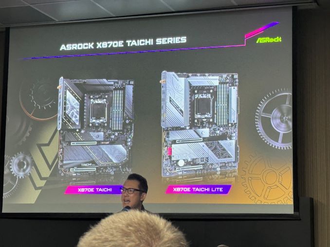

During Computex 2024, ASRock held an event to unveil some of its upcoming X870E motherboards, designed for AMD's Zen 5-based Ryzen 9000 series processors. ASRock's announcement includes a pair of Taichi-branded boards, the X870E Taichi and the lighter X870E Taichi lite, which uses AMD's X870E (Promontory 21) chipset for AM5.
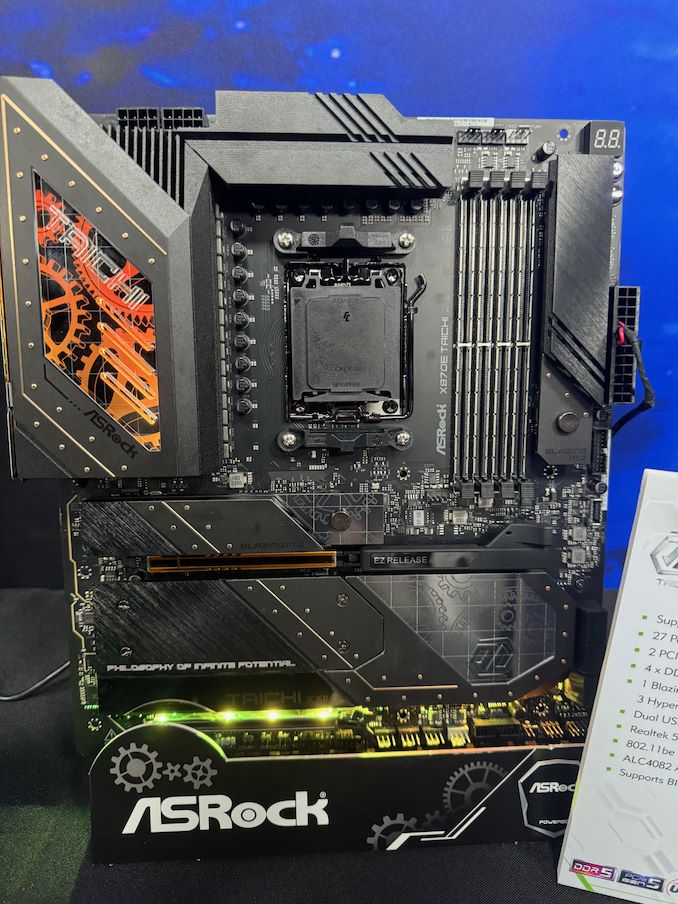
The current flagship model announced from ASRock's X870E line-up for Ryzen 9000 is the ASRock X870E Taichi. ASRock is advertising a large 27-phase power delivery through 110A SPS, suggesting this board is designed for overclockers and all-around power users. Two PCIe 5.0 x16 slots (operating in either x16/x0 or x8/x8) provide high-speed bandwidth for cutting-edge graphics cards and other devices. Meanwhile, ASRock has gone with 4 DIMM slots on this board, so system builders will be able to max out the board's memory capacity at the cost of bandwidth.
The storage offering is impressive; besides the obligatory PCIe Gen5 x4 M.2 slot (Blazing M.2), ASRock has outfit the board with another three PCIe Gen4 x4 (Hyper) M.2 slots. Also present are two USB4 Type-C ports for high-bandwidth external I/O, while networking support is a solid pairing of a discrete Wi-Fi 7 controller with a Realtek 5Gb Ethernet controller (and the first AM5 board we've come across with something faster than a 2.5GbE controller).
The audio setup includes a Realtek ALC4082 codec and ESS SABRE9218 DAC supporting high-fidelity sound. The BIOS flashback feature is also a nice touch, and we believe this should be a feature on all mid-range to high-end motherboards, which provides an easy way to update the firmware without installing a CPU. And, as no high-end board would be complete without it, ASRock has put RGB lighting on the X870E Taichi as well.
Ultimately, as ASRock's high-end X870E board, the X870E Taichi comes with pretty much every last cutting-edge technology that ASRock can fit on the board.
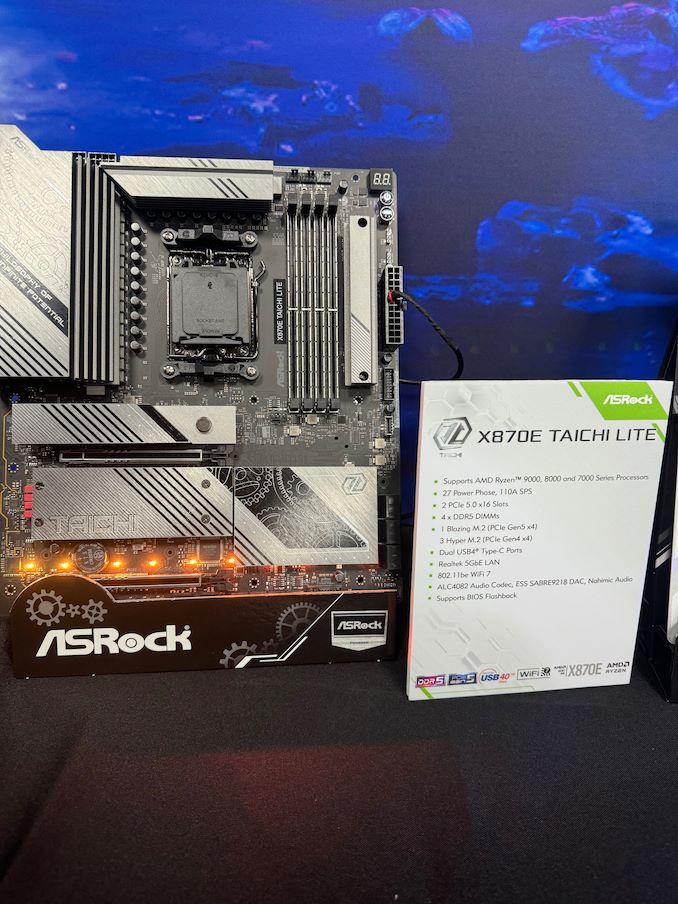
Comparatively, the ASRock X870E Taichi Lite is a more streamlined and functional version of the X870E Taichi. The Lite retaining all of the latter's key features, including the 27-phase power delivery with 110A smart power stages, dual PCIe 5.0 x16 slots operating at x16 or x8/x8, four DDR5 DIMM slots, and four M.2 slots (1x Gen5 + 3x Gen4). The only significant difference is aesthetics: the Taichi Lite features a simpler silver-themed design without the RGB lighting, while the standard Taichi has a more intricate gold-accented and fanciful aesthetics.
In terms of availability, ASRock is not disclosing a release date for the board at the show. And, checking around with other tech journalists, Andreas Schilling from HawrdwareLUXX has heard that X870E and X870 motherboards aren't expected to be available in time for the Ryzen 9000 series launch. We will investigate this and contact the motherboard vendors to confirm the situation. Though as X870E/X870 boards barely differ from the current crop of X670E/B650E boards to begin with, the Ryzen 9000 series won't be fazed by a lack of slightly newer motherboards.
Motherboards

Under the CHIPS & Science Act, the U.S. government provided tens of billions of dollars in grants and loans to the world's leading maker of chips, such as Intel, Samsung, and TSMC, which will significantly expand the country's semiconductor production industry in the coming years. However, most chips are typically tested, assembled, and packaged in Asia, which has left the American supply chain incomplete. Addressing this last gap in the government's domestic chip production plans, these past couple of weeks the U.S. government signed memorandums of understanding worth about $1.5 billion with Amkor and SK hynix to support their efforts to build chip packaging facilities in the U.S.
Amkor plans to build a $2 billion advanced packaging facility near Peoria, Arizona, to test and assemble chips produced by TSMC at its Fab 21 near Phoenix, Arizona. The company signed a MOU that offers $400 million in direct funding and access to $200 million in loans under the CHIPS & Science Act. In addition, the company plans to take advantage of a 25% investment tax credit on eligible capital expenditures.
Set to be strategically positioned near TSMC's upcoming Fab 21 complex in Arizona, Amkor's Peoria facility will occupy 55 acres and, when fully completed, will feature over 500,000 square feet (46,451 square meters) of cleanroom space, more than twice the size of Amkor's advanced packaging site in Vietnam. Although the company has not disclosed the exact capacity or the specific technologies the facility will support, it is expected to cater to a wide range of industries, including automotive, high-performance computing, and mobile technologies. This suggests the new plant will offer diverse packaging solutions, including traditional, 2.5D, and 3D technologies.
Amkor has collaborated extensively with Apple on the vision and initial setup of the Peoria facility, as Apple is slated to be the facility's first and largest customer, marking a significant commitment from the tech giant. This partnership highlights the importance of the new facility in reinforcing the U.S. semiconductor supply chain and positioning Amkor as a key partner for companies relying on TSMC's manufacturing capabilities. The project is expected to generate around 2,000 jobs and is scheduled to begin operations in 2027.
This week SK hynix also signed a preliminary agreement with the U.S. government to receive up to $450 million in direct funding and $500 million in loans to build an advanced memory packaging facility in West Lafayette, Indiana.
The proposed facility is scheduled to begin operations in 2028, which means that it will assemble HBM4 or HBM4E memory. Meanwhile, DRAM devices for high bandwidth memory (HBM) stacks will still be produced in South Korea. Nonetheless, packing finished HBM4/HBM4E in the U.S. and possibly integrating these memory modules with high-end processors is a big deal.
In addition to building its packaging plant, SK hynix plans to collaborate with Purdue University and other local research institutions to advance semiconductor technology and packaging innovations. This partnership is intended to bolster research and development in the region, positioning the facility as a hub for AI technology and skilled employment.
Semiconductors
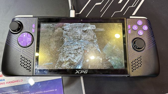
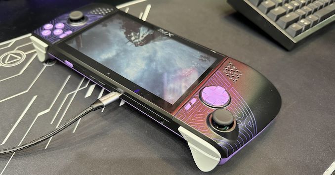
With the rise of the handheld gaming PC market, we've seen PC vendors and their partners toy with a number of tricks and tweaks to improve improve framerates in games, with some of their latest efforts on display at this year's Computex trade show. Perhaps the most interesting find thus far comes from ADATA sub-brand XPG, who is demoing their prototype "Nia" handheld PC, which uses eye tracking and dynamic foveated rendering to further improve their rendering performance.
For those unfamiliar, dynamic foveated rendering is a graphics technique that is sometimes used to boost performance in virtual reality (VR) and augmented reality (AR) applications by taking advantage of how human vision works. Typically, humans can only perceive detailed imagery in the relatively small central area of our vision called the fovea, while our peripheral vision is much less detailed. Dynamic foveated rendering, in turn, exploits this by using real-time eye tracking to determine where the user is looking, and then rendering just that area in high/full resolution, while rendering the peripheral areas in lower resolution. The net result is that only a fraction of the screen is rendered at full detail, which cuts down on the total amount of rendering work required and boosting framerates on performance-limited devices.
As stated before, this technology is sometimes used in high-end AR/VR headsets, where high resolution displays are placed mere inches from one's face. This ends up being an ideal use case for the technique, since at those distances, only a small fraction of the screen is within the fovea.
Using dynamic foveated rendering for a handheld, on the other hand, is a more novel application. All of the same visual principles apply, but the resolutions at play are lower, and the screen is farther from the users' eyes. This makes a handheld device a less ideal use case, at least on paper, as a larger portion of the screen is going to be in the fovea, and thus will need to be rendered at full resolution. None the less, it will be interesting to see how XPG's efforts pan out, and if dynamic foveated rendering is beneficial enough for handheld PCs. As we sometimes see with trade show demos, not everything makes it out of the prototype stage.
According to a press release put out by ADATA ahead of the trade show, the eye tracking technology is being provided by AMD collaborator Eyeware. Notably, their software-based approach runs on top of standard webcams, rather than requiring IR cameras. So the camera hardware itself should be pretty straight-forward.
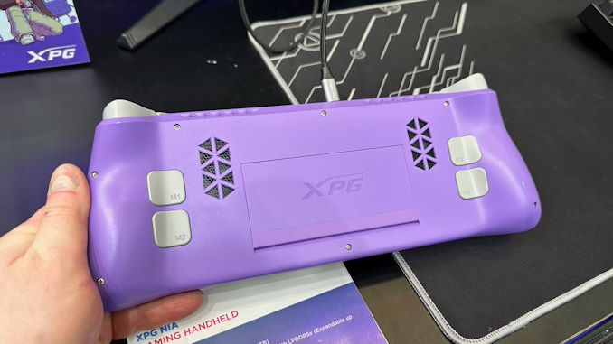
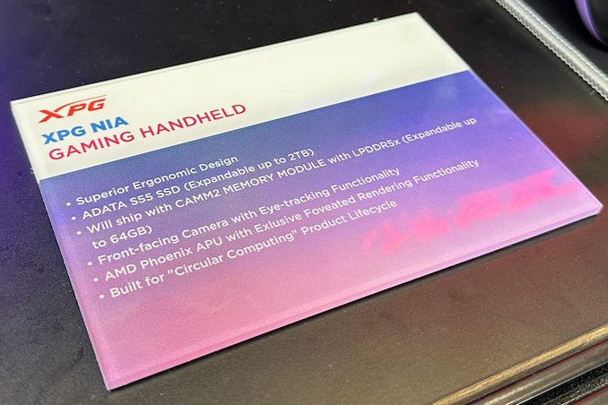
Foveated rendering aside, XPG is making sure that the Nia won't be a one-trick pony. The handheld's other major claim to fame is its hardware swappability. The prototype handheld not only features a removable M.2-2230 SSD, but the company is also taking advantage of the recently-introduced LPCAMM2 memory module standard to introduce removable DRAM. Via a hatch in the back of the handheld, device owners would be able to swap out LPCAMM2 LPDDR5X modules for higher capacity versions. This would give the handheld an additional degree of future-proofness over current handhelds, which use non-replaceable soldered-down memory.
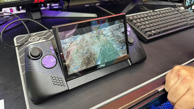
Rounding out the package, the current prototype is based on an AMD's Zen 4 Phoenix APU, which is used across both of the company's current mobile lines (Ryzen Mobile 7000/8000 and Ryzen Z1). Meanwhile, the unit's display is adjustable, allowing it to be angled away from the body of the handheld.
Assuming all goes well with the prototype, XPG aims to release a finished product in 2025.
Under the CHIPS & Science Act, the U.S. government provided tens of billions of dollars in grants and loans to the world's leading maker of chips, such as Intel, Samsung, and TSMC, which will significantly expand the country's semiconductor production industry in the coming years. However, most chips are typically tested, assembled, and packaged in Asia, which has left the American supply chain incomplete. Addressing this last gap in the government's domestic chip production plans, these past couple of weeks the U.S. government signed memorandums of understanding worth about $1.5 billion with Amkor and SK hynix to support their efforts to build chip packaging facilities in the U.S.
Amkor plans to build a $2 billion advanced packaging facility near Peoria, Arizona, to test and assemble chips produced by TSMC at its Fab 21 near Phoenix, Arizona. The company signed a MOU that offers $400 million in direct funding and access to $200 million in loans under the CHIPS & Science Act. In addition, the company plans to take advantage of a 25% investment tax credit on eligible capital expenditures.
Set to be strategically positioned near TSMC's upcoming Fab 21 complex in Arizona, Amkor's Peoria facility will occupy 55 acres and, when fully completed, will feature over 500,000 square feet (46,451 square meters) of cleanroom space, more than twice the size of Amkor's advanced packaging site in Vietnam. Although the company has not disclosed the exact capacity or the specific technologies the facility will support, it is expected to cater to a wide range of industries, including automotive, high-performance computing, and mobile technologies. This suggests the new plant will offer diverse packaging solutions, including traditional, 2.5D, and 3D technologies.
Amkor has collaborated extensively with Apple on the vision and initial setup of the Peoria facility, as Apple is slated to be the facility's first and largest customer, marking a significant commitment from the tech giant. This partnership highlights the importance of the new facility in reinforcing the U.S. semiconductor supply chain and positioning Amkor as a key partner for companies relying on TSMC's manufacturing capabilities. The project is expected to generate around 2,000 jobs and is scheduled to begin operations in 2027.
This week SK hynix also signed a preliminary agreement with the U.S. government to receive up to $450 million in direct funding and $500 million in loans to build an advanced memory packaging facility in West Lafayette, Indiana.
The proposed facility is scheduled to begin operations in 2028, which means that it will assemble HBM4 or HBM4E memory. Meanwhile, DRAM devices for high bandwidth memory (HBM) stacks will still be produced in South Korea. Nonetheless, packing finished HBM4/HBM4E in the U.S. and possibly integrating these memory modules with high-end processors is a big deal.
In addition to building its packaging plant, SK hynix plans to collaborate with Purdue University and other local research institutions to advance semiconductor technology and packaging innovations. This partnership is intended to bolster research and development in the region, positioning the facility as a hub for AI technology and skilled employment.
Semiconductors
With the rise of the handheld gaming PC market, we've seen PC vendors and their partners toy with a number of tricks and tweaks to improve improve framerates in games, with some of their latest efforts on display at this year's Computex trade show. Perhaps the most interesting find thus far comes from ADATA sub-brand XPG, who is demoing their prototype "Nia" handheld PC, which uses eye tracking and dynamic foveated rendering to further improve their rendering performance.
For those unfamiliar, dynamic foveated rendering is a graphics technique that is sometimes used to boost performance in virtual reality (VR) and augmented reality (AR) applications by taking advantage of how human vision works. Typically, humans can only perceive detailed imagery in the relatively small central area of our vision called the fovea, while our peripheral vision is much less detailed. Dynamic foveated rendering, in turn, exploits this by using real-time eye tracking to determine where the user is looking, and then rendering just that area in high/full resolution, while rendering the peripheral areas in lower resolution. The net result is that only a fraction of the screen is rendered at full detail, which cuts down on the total amount of rendering work required and boosting framerates on performance-limited devices.
As stated before, this technology is sometimes used in high-end AR/VR headsets, where high resolution displays are placed mere inches from one's face. This ends up being an ideal use case for the technique, since at those distances, only a small fraction of the screen is within the fovea.
Using dynamic foveated rendering for a handheld, on the other hand, is a more novel application. All of the same visual principles apply, but the resolutions at play are lower, and the screen is farther from the users' eyes. This makes a handheld device a less ideal use case, at least on paper, as a larger portion of the screen is going to be in the fovea, and thus will need to be rendered at full resolution. None the less, it will be interesting to see how XPG's efforts pan out, and if dynamic foveated rendering is beneficial enough for handheld PCs. As we sometimes see with trade show demos, not everything makes it out of the prototype stage.
According to a press release put out by ADATA ahead of the trade show, the eye tracking technology is being provided by AMD collaborator Eyeware. Notably, their software-based approach runs on top of standard webcams, rather than requiring IR cameras. So the camera hardware itself should be pretty straight-forward.
Foveated rendering aside, XPG is making sure that the Nia won't be a one-trick pony. The handheld's other major claim to fame is its hardware swappability. The prototype handheld not only features a removable M.2-2230 SSD, but the company is also taking advantage of the recently-introduced LPCAMM2 memory module standard to introduce removable DRAM. Via a hatch in the back of the handheld, device owners would be able to swap out LPCAMM2 LPDDR5X modules for higher capacity versions. This would give the handheld an additional degree of future-proofness over current handhelds, which use non-replaceable soldered-down memory.
Rounding out the package, the current prototype is based on an AMD's Zen 4 Phoenix APU, which is used across both of the company's current mobile lines (Ryzen Mobile 7000/8000 and Ryzen Z1). Meanwhile, the unit's display is adjustable, allowing it to be angled away from the body of the handheld.
Assuming all goes well with the prototype, XPG aims to release a finished product in 2025.

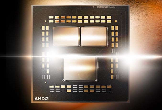
During their opening keynote at Computex 2024, AMD announced their intention to launch a pair of new Ryzen 5000 processors for their legacy AM4 platform. The new chips, both getting the XT suffix, will be the Ryzen 9 5900XT, a 16 core Zen 3 part, while the Ryzen 7 5800XT will be an 8 core Zen 3.
The new chips are intended to underscore AMD's ongoing commitment to supporting their consumer platforms over several years. And while the specification changes are rather minor overall – the Zen 3 CPU architecture has long since been taken as far as it can reasonable go – it does give AMD a chance to refresh the platform by slinging hardware at new price points. AMD did something very similar for the Ryzen 3000 generation with the late-model Ryzen 3000 XT chips.
| AMD Ryzen 5000XT Series Processors (Zen 3) |
||||||
| AnandTech | Cores / Threads |
Base Freq |
Turbo Freq |
L2 Cache |
L3 Cache |
TDP |
| Ryzen 9 5950X | 16C / 32T | 3.4 GHz | 4.9 GHz | 8 MB | 64 MB | 105 W |
| Ryzen 9 5900XT | 16C / 32T | 3.3 GHz | 4.8 GHz | 8 MB | 64 MB | 105 W |
| Ryzen 9 5900X | 12C / 24T | 3.7 GHz | 4.8 GHz | 6 MB | 64 MB | 105 W |
| Ryzen 7 5800XT | 8C / 16T | 3.8 GHz | 4.8 GHz | 4 MB | 32 MB | 105 W |
| Ryzen 7 5800X | 8C / 16T | 3.8 GHz | 4.7 GHz | 4 MB | 32 MB | 105 W |
We've dedicated many column inches covering Zen 3 and the Ryzen 5000 series since they launched in late 2020, so there isn't anything new to add here. Zen 3 is no longer AMD's latest and greatest, but the platform as a whole is quite cheap to produce, making it a viable budget offering for new builds, or offering one last upgrade for old builds.
The Ryzen 9 5900XT is a 16 core part, and isn't to be confused with the Ryzen 9 5900X, which is a 12 core part. It ships with a peak turbo clockspeed of 4.8GHz, 100 MHz lower than the top-tier Ryzen 9 5950X. This makes it's XT designation somewhat of a misnomer compared to previous generations of XT chips, although it's clear that AMD has boxed themselves into a corner with their naming scheme, as they both need a way to designate that this is a new chip, and yet still place it below the 5950X.
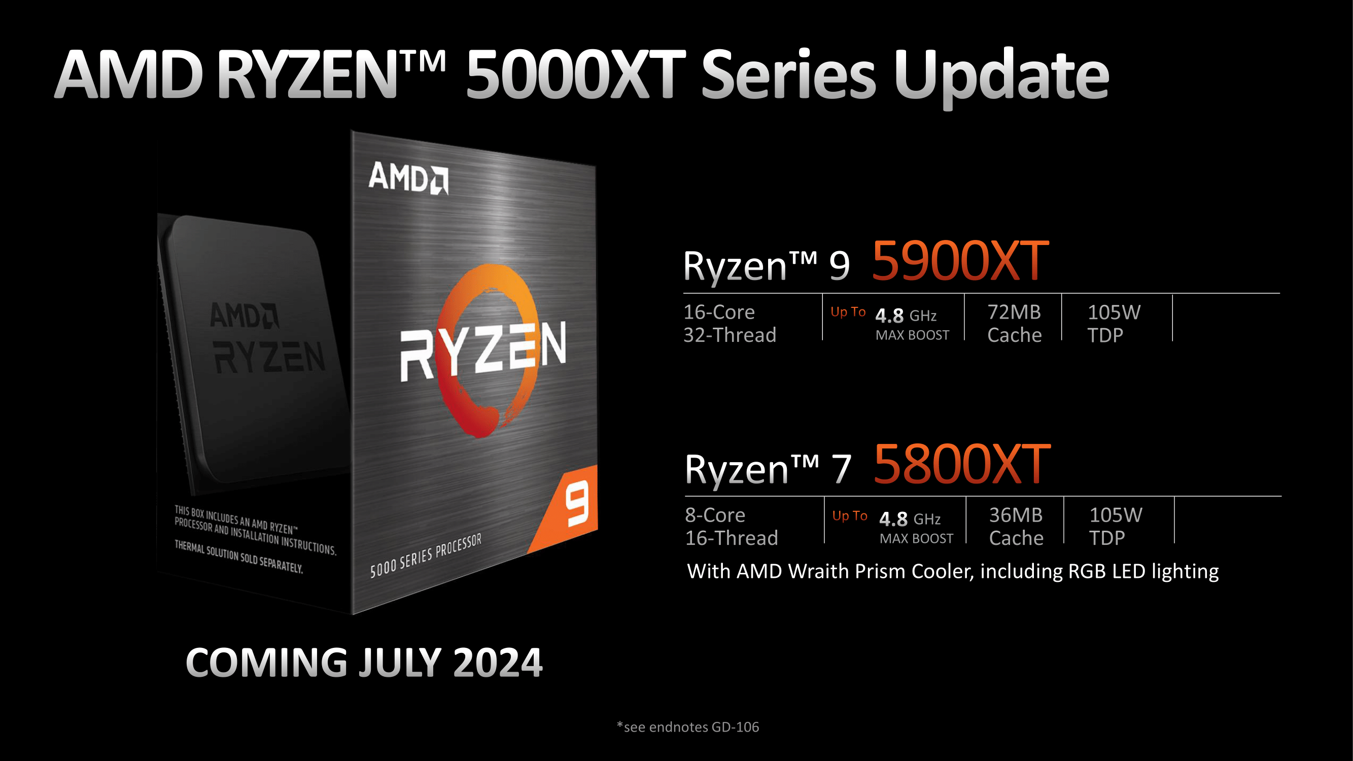
Looking at the second chip, we have the Ryzen 7 5800XT. This is an 8 core part that does improve on its predecessor, offering a 4.8GHz max turbo clock that is 100MHz higher than the Ryzen 7 5800X's. Both chips otherwise share the same characteristics, including 6 MB of L2 cache and 32 MB of L3 cache, and all four of the chips – including the two new XT series and the corresponding X series chips – all come with a 105 Watt TDP.
In terms of motherboard compatibility, all of the AM4 motherboards that currently support the Ryzen 5000 series are also compatible with the Ryzen 5000XT series, although users are likely to need to perform a firmware update to ensure maximum compatibility; they are the same chips, but the microcodes are likely different.
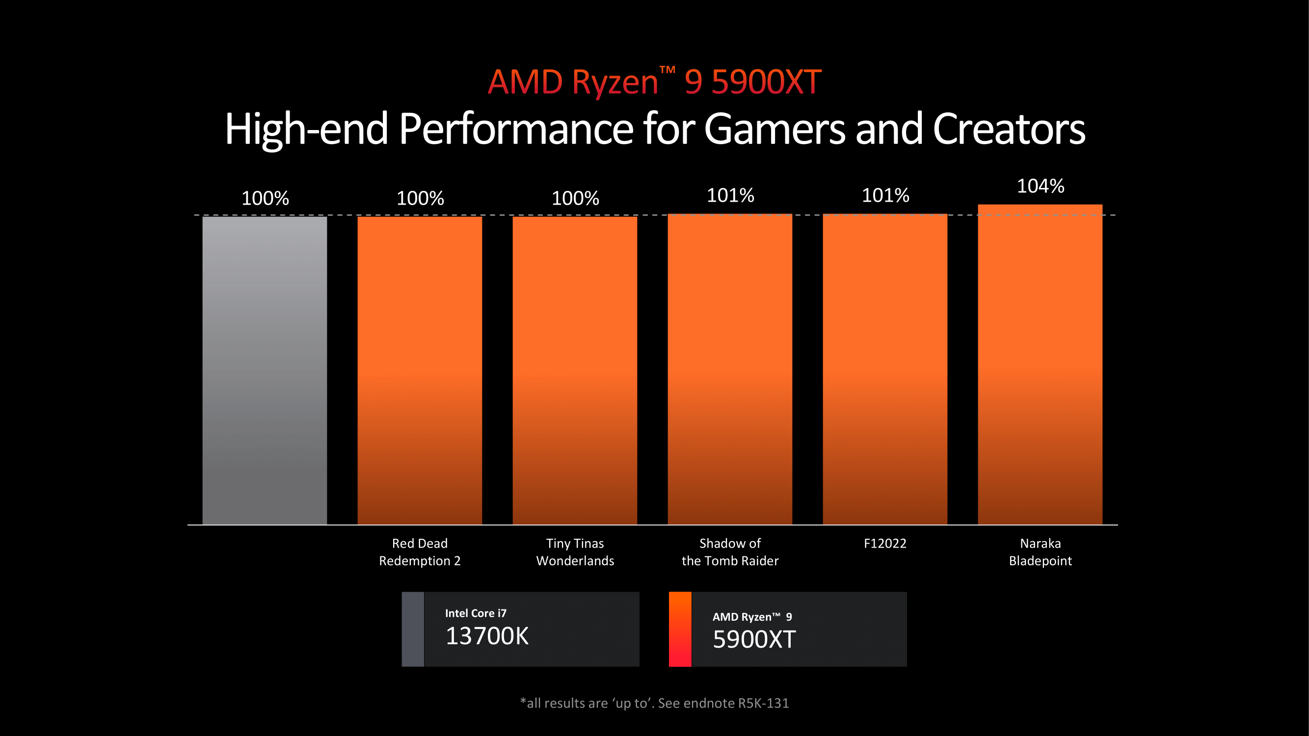
AMD has provided some gaming performance figures comparing the Ryzen 9 5900XT to Intel's 13th Gen Core i7-13700K. It does offer very modest yet marginal gains in games by up to 4%; it's not mind-blowing, but the... CPUs

Lorem Ipsum is simply dummy text of the printing and typesetting industry. Lorem Ipsum has been the industry's.
Under the CHIPS & Science Act, the U.S. government provided tens of billions of dollars in grants and loans to the world's leading maker of chips, such as Intel, Samsung, and TSMC, which will significantly expand the country's semiconductor production industry in the coming years. However, most chips are typically tested, assembled, and packaged in Asia, which has left the American supply chain incomplete. Addressing this last gap in the government's domestic chip production plans, these past couple of weeks the U.S. government signed memorandums of understanding worth about $1.5 billion with Amkor and SK hynix to support their efforts to build chip packaging facilities in the U.S.
Amkor plans to build a $2 billion advanced packaging facility near Peoria, Arizona, to test and assemble chips produced by TSMC at its Fab 21 near Phoenix, Arizona. The company signed a MOU that offers $400 million in direct funding and access to $200 million in loans under the CHIPS & Science Act. In addition, the company plans to take advantage of a 25% investment tax credit on eligible capital expenditures.
Set to be strategically positioned near TSMC's upcoming Fab 21 complex in Arizona, Amkor's Peoria facility will occupy 55 acres and, when fully completed, will feature over 500,000 square feet (46,451 square meters) of cleanroom space, more than twice the size of Amkor's advanced packaging site in Vietnam. Although the company has not disclosed the exact capacity or the specific technologies the facility will support, it is expected to cater to a wide range of industries, including automotive, high-performance computing, and mobile technologies. This suggests the new plant will offer diverse packaging solutions, including traditional, 2.5D, and 3D technologies.
Amkor has collaborated extensively with Apple on the vision and initial setup of the Peoria facility, as Apple is slated to be the facility's first and largest customer, marking a significant commitment from the tech giant. This partnership highlights the importance of the new facility in reinforcing the U.S. semiconductor supply chain and positioning Amkor as a key partner for companies relying on TSMC's manufacturing capabilities. The project is expected to generate around 2,000 jobs and is scheduled to begin operations in 2027.
This week SK hynix also signed a preliminary agreement with the U.S. government to receive up to $450 million in direct funding and $500 million in loans to build an advanced memory packaging facility in West Lafayette, Indiana.
The proposed facility is scheduled to begin operations in 2028, which means that it will assemble HBM4 or HBM4E memory. Meanwhile, DRAM devices for high bandwidth memory (HBM) stacks will still be produced in South Korea. Nonetheless, packing finished HBM4/HBM4E in the U.S. and possibly integrating these memory modules with high-end processors is a big deal.
In addition to building its packaging plant, SK hynix plans to collaborate with Purdue University and other local research institutions to advance semiconductor technology and packaging innovations. This partnership is intended to bolster research and development in the region, positioning the facility as a hub for AI technology and skilled employment.
Semiconductors


 chipset for AM5.</p>
<p align="center"><a href="https://www.anandtech.com/show/21433/asrock-unveils-motherboards-for-ryzen-9000-at-computex-2024-x870e-taichi-and-x870e-taichi-lite"><img alt="" src="https://images.anandtech.com/doci/21433/IMG_1865_575px.jpg" /></a></p>
<p>The current flagship model announced from ASRock's X870E line-up for Ryzen 9000 is the ASRock X870E Taichi. ASRock is advertising a large 27-phase power delivery through 110A SPS, suggesting this board is designed for overclockers and all-around power users. Two PCIe 5.0 x16 slots (operating in either x16/x0 or x8/x8) provide high-speed bandwidth for cutting-edge graphics cards and other devices. Meanwhile, ASRock has gone with 4 DIMM slots on this board, so system builders will be able to max out the board's memory capacity at the cost of bandwidth.</p>
<p>The storage offering is impressive; besides the obligatory PCIe Gen5 x4 M.2 slot (Blazing M.2), ASRock has outfit the board with another three PCIe Gen4 x4 (Hyper) M.2 slots. Also present are two USB4 Type-C ports for high-bandwidth external I/O, while networking support is a solid pairing of a discrete Wi-Fi 7 controller with a Realtek 5Gb Ethernet controller (and the first AM5 board we've come across with something faster than a 2.5GbE controller).</p>
<p>The audio setup includes a Realtek ALC4082 codec and ESS SABRE9218 DAC supporting high-fidelity sound. The BIOS flashback feature is also a nice touch, and we believe this should be a feature on all mid-range to high-end motherboards, which provides an easy way to update the firmware without installing a CPU. And, as no high-end board would be complete without it, ASRock has put RGB lighting on the X870E Taichi as well.</p>
<p>Ultimately, as ASRock's high-end X870E board, the X870E Taichi comes with pretty much every last cutting-edge technology that ASRock can fit on the board.</p>
<p align="center"><a href="https://www.anandtech.com/show/21433/asrock-unveils-motherboards-for-ryzen-9000-at-computex-2024-x870e-taichi-and-x870e-taichi-lite"><img alt="" src="https://images.anandtech.com/doci/21433/IMG_1866_575px.jpg" /></a></p>
<p>Comparatively, the ASRock X870E Taichi Lite is a more streamlined and functional version of the X870E Taichi. The Lite retaining all of the latter's key features, including the 27-phase power delivery with 110A smart power stages, dual PCIe 5.0 x16 slots operating at x16 or x8/x8, four DDR5 DIMM slots, and four M.2 slots (1x Gen5 + 3x Gen4). The only significant difference is aesthetics: the Taichi Lite features a simpler silver-themed design without the RGB lighting, while the standard Taichi has a more intricate gold-accented and fanciful aesthetics.</p>
<p>In terms of availability, ASRock is not disclosing a release date for the board at the show. And, checking around with other tech journalists, <a href="https://www.hardwareluxx.de/index.php/news/hardware/mainboards/63788-amd-ryzen-9000-x870-und-x870e-boards-kommen-nach-dem-start-der-prozessoren.html">Andreas Schilling from HawrdwareLUXX</a> has heard that X870E and X870 motherboards aren't expected to be available in time for the Ryzen 9000 series launch. We will investigate this and contact the motherboard vendors to confirm the situation. Though as X870E/X870 boards barely differ from the current crop of X670E/B650E boards to begin with, the Ryzen 9000 series won't be fazed by a lack of slightly newer motherboards.</p>
</p> Motherboards)
 chipset for AM5.</p>
<p align="center"><a href="https://www.anandtech.com/show/21433/asrock-unveils-motherboards-for-ryzen-9000-at-computex-2024-x870e-taichi-and-x870e-taichi-lite"><img alt="" src="https://images.anandtech.com/doci/21433/IMG_1865_575px.jpg" /></a></p>
<p>The current flagship model announced from ASRock's X870E line-up for Ryzen 9000 is the ASRock X870E Taichi. ASRock is advertising a large 27-phase power delivery through 110A SPS, suggesting this board is designed for overclockers and all-around power users. Two PCIe 5.0 x16 slots (operating in either x16/x0 or x8/x8) provide high-speed bandwidth for cutting-edge graphics cards and other devices. Meanwhile, ASRock has gone with 4 DIMM slots on this board, so system builders will be able to max out the board's memory capacity at the cost of bandwidth.</p>
<p>The storage offering is impressive; besides the obligatory PCIe Gen5 x4 M.2 slot (Blazing M.2), ASRock has outfit the board with another three PCIe Gen4 x4 (Hyper) M.2 slots. Also present are two USB4 Type-C ports for high-bandwidth external I/O, while networking support is a solid pairing of a discrete Wi-Fi 7 controller with a Realtek 5Gb Ethernet controller (and the first AM5 board we've come across with something faster than a 2.5GbE controller).</p>
<p>The audio setup includes a Realtek ALC4082 codec and ESS SABRE9218 DAC supporting high-fidelity sound. The BIOS flashback feature is also a nice touch, and we believe this should be a feature on all mid-range to high-end motherboards, which provides an easy way to update the firmware without installing a CPU. And, as no high-end board would be complete without it, ASRock has put RGB lighting on the X870E Taichi as well.</p>
<p>Ultimately, as ASRock's high-end X870E board, the X870E Taichi comes with pretty much every last cutting-edge technology that ASRock can fit on the board.</p>
<p align="center"><a href="https://www.anandtech.com/show/21433/asrock-unveils-motherboards-for-ryzen-9000-at-computex-2024-x870e-taichi-and-x870e-taichi-lite"><img alt="" src="https://images.anandtech.com/doci/21433/IMG_1866_575px.jpg" /></a></p>
<p>Comparatively, the ASRock X870E Taichi Lite is a more streamlined and functional version of the X870E Taichi. The Lite retaining all of the latter's key features, including the 27-phase power delivery with 110A smart power stages, dual PCIe 5.0 x16 slots operating at x16 or x8/x8, four DDR5 DIMM slots, and four M.2 slots (1x Gen5 + 3x Gen4). The only significant difference is aesthetics: the Taichi Lite features a simpler silver-themed design without the RGB lighting, while the standard Taichi has a more intricate gold-accented and fanciful aesthetics.</p>
<p>In terms of availability, ASRock is not disclosing a release date for the board at the show. And, checking around with other tech journalists, <a href="https://www.hardwareluxx.de/index.php/news/hardware/mainboards/63788-amd-ryzen-9000-x870-und-x870e-boards-kommen-nach-dem-start-der-prozessoren.html">Andreas Schilling from HawrdwareLUXX</a> has heard that X870E and X870 motherboards aren't expected to be available in time for the Ryzen 9000 series launch. We will investigate this and contact the motherboard vendors to confirm the situation. Though as X870E/X870 boards barely differ from the current crop of X670E/B650E boards to begin with, the Ryzen 9000 series won't be fazed by a lack of slightly newer motherboards.</p>
</p> Motherboards)
 chipset for AM5.</p>
<p align="center"><a href="https://www.anandtech.com/show/21433/asrock-unveils-motherboards-for-ryzen-9000-at-computex-2024-x870e-taichi-and-x870e-taichi-lite"><img alt="" src="https://images.anandtech.com/doci/21433/IMG_1865_575px.jpg" /></a></p>
<p>The current flagship model announced from ASRock's X870E line-up for Ryzen 9000 is the ASRock X870E Taichi. ASRock is advertising a large 27-phase power delivery through 110A SPS, suggesting this board is designed for overclockers and all-around power users. Two PCIe 5.0 x16 slots (operating in either x16/x0 or x8/x8) provide high-speed bandwidth for cutting-edge graphics cards and other devices. Meanwhile, ASRock has gone with 4 DIMM slots on this board, so system builders will be able to max out the board's memory capacity at the cost of bandwidth.</p>
<p>The storage offering is impressive; besides the obligatory PCIe Gen5 x4 M.2 slot (Blazing M.2), ASRock has outfit the board with another three PCIe Gen4 x4 (Hyper) M.2 slots. Also present are two USB4 Type-C ports for high-bandwidth external I/O, while networking support is a solid pairing of a discrete Wi-Fi 7 controller with a Realtek 5Gb Ethernet controller (and the first AM5 board we've come across with something faster than a 2.5GbE controller).</p>
<p>The audio setup includes a Realtek ALC4082 codec and ESS SABRE9218 DAC supporting high-fidelity sound. The BIOS flashback feature is also a nice touch, and we believe this should be a feature on all mid-range to high-end motherboards, which provides an easy way to update the firmware without installing a CPU. And, as no high-end board would be complete without it, ASRock has put RGB lighting on the X870E Taichi as well.</p>
<p>Ultimately, as ASRock's high-end X870E board, the X870E Taichi comes with pretty much every last cutting-edge technology that ASRock can fit on the board.</p>
<p align="center"><a href="https://www.anandtech.com/show/21433/asrock-unveils-motherboards-for-ryzen-9000-at-computex-2024-x870e-taichi-and-x870e-taichi-lite"><img alt="" src="https://images.anandtech.com/doci/21433/IMG_1866_575px.jpg" /></a></p>
<p>Comparatively, the ASRock X870E Taichi Lite is a more streamlined and functional version of the X870E Taichi. The Lite retaining all of the latter's key features, including the 27-phase power delivery with 110A smart power stages, dual PCIe 5.0 x16 slots operating at x16 or x8/x8, four DDR5 DIMM slots, and four M.2 slots (1x Gen5 + 3x Gen4). The only significant difference is aesthetics: the Taichi Lite features a simpler silver-themed design without the RGB lighting, while the standard Taichi has a more intricate gold-accented and fanciful aesthetics.</p>
<p>In terms of availability, ASRock is not disclosing a release date for the board at the show. And, checking around with other tech journalists, <a href="https://www.hardwareluxx.de/index.php/news/hardware/mainboards/63788-amd-ryzen-9000-x870-und-x870e-boards-kommen-nach-dem-start-der-prozessoren.html">Andreas Schilling from HawrdwareLUXX</a> has heard that X870E and X870 motherboards aren't expected to be available in time for the Ryzen 9000 series launch. We will investigate this and contact the motherboard vendors to confirm the situation. Though as X870E/X870 boards barely differ from the current crop of X670E/B650E boards to begin with, the Ryzen 9000 series won't be fazed by a lack of slightly newer motherboards.</p>
</p> Motherboards | https://compbuddey.blogspot.com/2024/06/asrock-unveils-motherboards-for-ryzen_17.html)
 chipset for AM5.</p>
<p align="center"><a href="https://www.anandtech.com/show/21433/asrock-unveils-motherboards-for-ryzen-9000-at-computex-2024-x870e-taichi-and-x870e-taichi-lite"><img alt="" src="https://images.anandtech.com/doci/21433/IMG_1865_575px.jpg" /></a></p>
<p>The current flagship model announced from ASRock's X870E line-up for Ryzen 9000 is the ASRock X870E Taichi. ASRock is advertising a large 27-phase power delivery through 110A SPS, suggesting this board is designed for overclockers and all-around power users. Two PCIe 5.0 x16 slots (operating in either x16/x0 or x8/x8) provide high-speed bandwidth for cutting-edge graphics cards and other devices. Meanwhile, ASRock has gone with 4 DIMM slots on this board, so system builders will be able to max out the board's memory capacity at the cost of bandwidth.</p>
<p>The storage offering is impressive; besides the obligatory PCIe Gen5 x4 M.2 slot (Blazing M.2), ASRock has outfit the board with another three PCIe Gen4 x4 (Hyper) M.2 slots. Also present are two USB4 Type-C ports for high-bandwidth external I/O, while networking support is a solid pairing of a discrete Wi-Fi 7 controller with a Realtek 5Gb Ethernet controller (and the first AM5 board we've come across with something faster than a 2.5GbE controller).</p>
<p>The audio setup includes a Realtek ALC4082 codec and ESS SABRE9218 DAC supporting high-fidelity sound. The BIOS flashback feature is also a nice touch, and we believe this should be a feature on all mid-range to high-end motherboards, which provides an easy way to update the firmware without installing a CPU. And, as no high-end board would be complete without it, ASRock has put RGB lighting on the X870E Taichi as well.</p>
<p>Ultimately, as ASRock's high-end X870E board, the X870E Taichi comes with pretty much every last cutting-edge technology that ASRock can fit on the board.</p>
<p align="center"><a href="https://www.anandtech.com/show/21433/asrock-unveils-motherboards-for-ryzen-9000-at-computex-2024-x870e-taichi-and-x870e-taichi-lite"><img alt="" src="https://images.anandtech.com/doci/21433/IMG_1866_575px.jpg" /></a></p>
<p>Comparatively, the ASRock X870E Taichi Lite is a more streamlined and functional version of the X870E Taichi. The Lite retaining all of the latter's key features, including the 27-phase power delivery with 110A smart power stages, dual PCIe 5.0 x16 slots operating at x16 or x8/x8, four DDR5 DIMM slots, and four M.2 slots (1x Gen5 + 3x Gen4). The only significant difference is aesthetics: the Taichi Lite features a simpler silver-themed design without the RGB lighting, while the standard Taichi has a more intricate gold-accented and fanciful aesthetics.</p>
<p>In terms of availability, ASRock is not disclosing a release date for the board at the show. And, checking around with other tech journalists, <a href="https://www.hardwareluxx.de/index.php/news/hardware/mainboards/63788-amd-ryzen-9000-x870-und-x870e-boards-kommen-nach-dem-start-der-prozessoren.html">Andreas Schilling from HawrdwareLUXX</a> has heard that X870E and X870 motherboards aren't expected to be available in time for the Ryzen 9000 series launch. We will investigate this and contact the motherboard vendors to confirm the situation. Though as X870E/X870 boards barely differ from the current crop of X670E/B650E boards to begin with, the Ryzen 9000 series won't be fazed by a lack of slightly newer motherboards.</p>
</p> Motherboards&body=https://compbuddey.blogspot.com/2024/06/asrock-unveils-motherboards-for-ryzen_17.html)


0 Comments