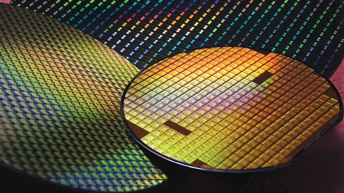

At its European Technology Symposium last week TSMC revealed some of the details about its Global Gigafab Manufacturing program, the company's strategy to replicate its manufacturing processes across its multiple gigafab sites.
The need for large-scale multi-national fabs to have a process in place to replicate their facilities is well-documented at this point. As scaling-up at at the gigafab size means scaling-out instead, chip makers need to be able to quickly get new and updated manufacturing processes ported to other facilities in order to hit their necessary throughput – and to avoid a multi-quarter bottlenecks that come from having to freshly-tune a fab.
Intel, for their part, has a well-known Copy Exactly program, which is one of the company's major competitive advantages, allowing it to share process recipes across its fabs around the world to maximize yields and reduce performance variability. Meanwhile, as Taiwan Semiconductor Manufacturing Co. is building additional capacity in different parts of the world, it has reached the point where it needs a similar program in order to quickly maximize its yields and productivity at its new fabs in Japan and the U.S. And in some respects, TSMC's program goes even further than Intel's, with an additional focus on sustainability and social responsibility.
"As mentioned at last year's symposium, [Global Gigafab manufacturing] is a powerful global manufacturing and management platform," said Y.L. Wang, Vice President of Fab Operations TSMC. "We realise one fab management to ensure our Gigafab to achieve consistent operation efficiency as well as production quality on a global scale. Moreover, we also pursue sustainability across our global footprint covering green manufacturing, global talent development, supply chain localization, as well as social responsibility."
| TSMC's Global GigaFab Manufacturing Data by TSMC (Compiled by AnandTech) |
|||
| Manufacturing Excellence | Sustainability | ||
| Global One Fab Manufacturing | Green Manufacturing | ||
| ML-based Process Control | Global Talent Development | ||
| Manufacturing Agility and Quality | Supply Chain Localization | ||
| Maximum Productivity | Social Responsibility | ||
When it comes to improvements of process technology, there are two main mechanisms: the continuous process improvements (CPI) to improve yields, as well as statistical process control (SPC) reduce performance variations. To do so, the company has multiple internal techniques that rely on machine learning-based process control, constant quality measuring, and various productivity improving methods. With Global Gigafab manufacturing TSMC can use CPI and SPC to improve yields and performance on the global scale by sharing knowledge between different sites.
"When we port a technology from Taiwan to Arizona, the fab set up, the process control system, everything is actually a copy from Taiwan," said Kevin Zhang, Senior Vice President, Business Development and Overseas Operations Office, and Deputy Co-COO at TSMC.
TSMC yet has to start making chips at its fabs in Germany, Japan, and the United States, so it remains to be seen how fast the foundry will increase yields to Taiwanese levels at its Fab 23 (in Kumamoto, Japan) and Fab 21 (in Arizona) when they begin operations in 2024 and 2025, but with Global Gigafab Manufacturing program in place, this is likely set to happen rather sooner than later.
Semiconductors

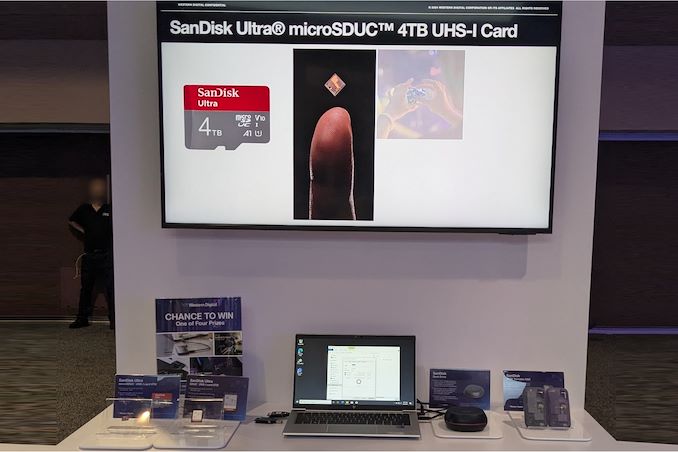
Western Digital's BiCS8 218-layer 3D NAND is being put to good use in a wide range of client and enterprise platforms, including WD's upcoming Gen 5 client SSDs and 128 TB-class datacenter SSD. On the external storage front, the company demonstrated four different products: for card-based media, 4 TB microSDUC and 8 TB SDUC cards with UHS-I speeds, and on the portable SSD front we had two 16 TB drives. One will be a SanDisk Desk Drive with external power, and the other in the SanDisk Extreme Pro housing with a lanyard opening in the case.
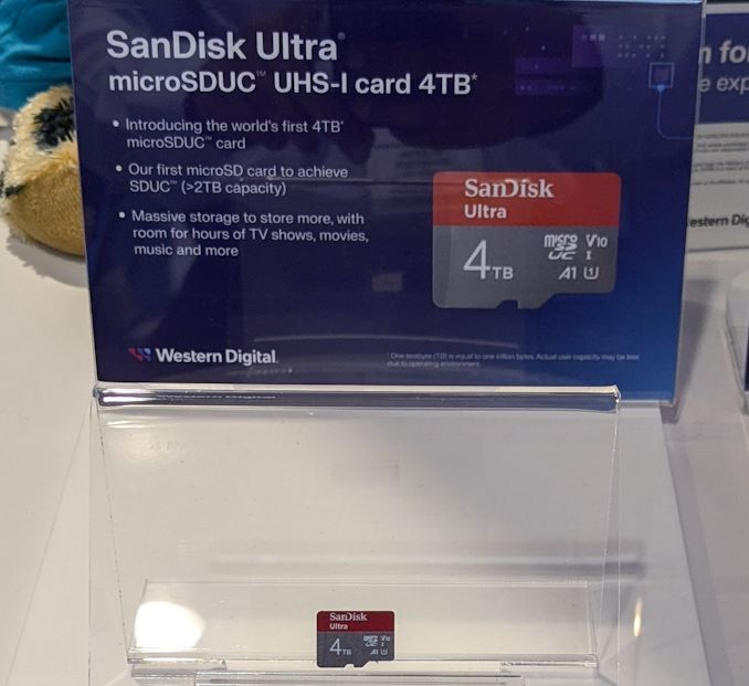
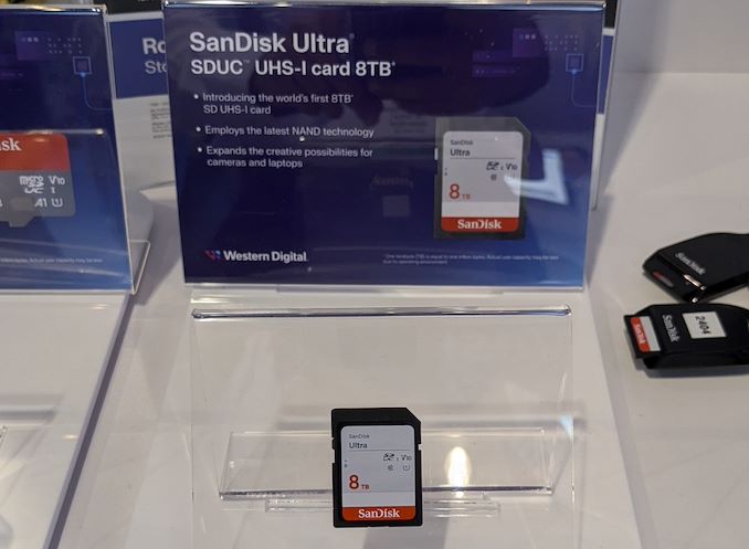
All of these are using BiCS8 QLC NAND, though I did hear booth talk (as I was taking leave) that they were not supposed to divulge the use of QLC in these products. The 4 TB microSDUC and 8 TB SDUC cards are rated for UHS-I speeds. They are being marketed under the SanDisk Ultra branding.
The SanDisk Desk Drive is an external SSD with a 18W power adapter, and it has been in the market for a few months now. Initially launched in capacities up to 8 TB, Western Digital had promised a 16 TB version before the end of the year. It appears that the product is coming to retail quite soon. One aspect to note is that this drive has been using TLC for the SKUs that are currently in the market, so it appears unlikely that the 16 TB version would be QLC. The units (at least up to the 8 TB capacity point) come with two SN850XE drives. Given the recent introduction of the 8 TB SN850X, an 'E' version with tweaked firmware is likely to be present in the 16 TB Desk Drive.
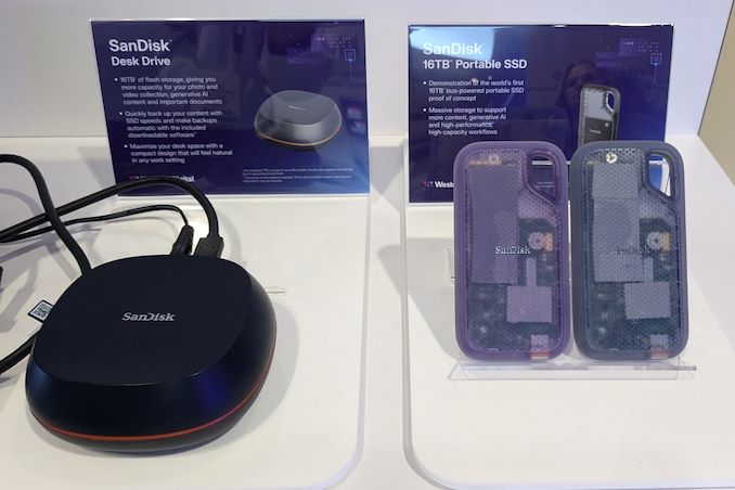
The 16 TB portable SSD in the SanDisk Extreme housing was a technology demonstration. It is definitely the highest capacity bus-powered portable SSD demonstrated by any vendor at any trade show thus far. Given the 16 TB Desk Drive's imminent market introduction, it is just a matter of time before the technology demonstration of the bus-powered version becomes a retail reality.
Storage
Western Digital's BiCS8 218-layer 3D NAND is being put to good use in a wide range of client and enterprise platforms, including WD's upcoming Gen 5 client SSDs and 128 TB-class datacenter SSD. On the external storage front, the company demonstrated four different products: for card-based media, 4 TB microSDUC and 8 TB SDUC cards with UHS-I speeds, and on the portable SSD front we had two 16 TB drives. One will be a SanDisk Desk Drive with external power, and the other in the SanDisk Extreme Pro housing with a lanyard opening in the case.
All of these are using BiCS8 QLC NAND, though I did hear booth talk (as I was taking leave) that they were not supposed to divulge the use of QLC in these products. The 4 TB microSDUC and 8 TB SDUC cards are rated for UHS-I speeds. They are being marketed under the SanDisk Ultra branding.
The SanDisk Desk Drive is an external SSD with a 18W power adapter, and it has been in the market for a few months now. Initially launched in capacities up to 8 TB, Western Digital had promised a 16 TB version before the end of the year. It appears that the product is coming to retail quite soon. One aspect to note is that this drive has been using TLC for the SKUs that are currently in the market, so it appears unlikely that the 16 TB version would be QLC. The units (at least up to the 8 TB capacity point) come with two SN850XE drives. Given the recent introduction of the 8 TB SN850X, an 'E' version with tweaked firmware is likely to be present in the 16 TB Desk Drive.
The 16 TB portable SSD in the SanDisk Extreme housing was a technology demonstration. It is definitely the highest capacity bus-powered portable SSD demonstrated by any vendor at any trade show thus far. Given the 16 TB Desk Drive's imminent market introduction, it is just a matter of time before the technology demonstration of the bus-powered version becomes a retail reality.
Storage
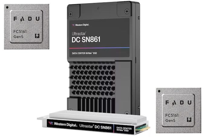
When Western Digital introduced its Ultrastar DC SN861 SSDs earlier this year, the company did not disclose which controller it used for these drives, which made many observers presume that WD was using an in-house controller. But a recent teardown of the drive shows that is not the case; instead, the company is using a controller from Fadu, a South Korean company founded in 2015 that specializes on enterprise-grade turnkey SSD solutions.
The Western Digital Ultrastar DC SN861 SSD is aimed at performance-hungry hyperscale datacenters and enterprise customers which are adopting PCIe Gen5 storage devices these days. And, as uncovered in photos from a recent Storage Review article, the drive is based on Fadu's FC5161 NVMe 2.0-compliant controller. The FC5161 utilizes 16 NAND channels supporting an ONFi 5.0 2400 MT/s interface, and features a combination of enterprise-grade capabilities (OCP Cloud Spec 2.0, SR-IOV, up to 512 name spaces for ZNS support, flexible data placement, NVMe-MI 1.2, advanced security, telemetry, power loss protection) not available on other off-the-shelf controllers – or on any previous Western Digital controllers.
The Ultrastar DC SN861 SSD offers sequential read speeds up to 13.7 GB/s as well as sequential write speeds up to 7.5 GB/s. As for random performance, it boasts with an up to 3.3 million random 4K read IOPS and up to 0.8 million random 4K write IOPS. The drives are available in capacities between 1.6 TB and 7.68 TB with one or three drive writes per day (DWPD) over five years rating as well as in U.2 and E1.S form-factors.
While the two form factors of the SN861 share a similar technical design, Western Digital has tailored each version for distinct workloads: the E1.S supports FDP and performance enhancements specifically for cloud environments. By contrast, the U.2 model is geared towards high-performance enterprise tasks and emerging applications like AI.
Without any doubts, Western Digital's Ultrastar DC SN861 is a feature-rich high-performance enterprise-grade SSD. It has another distinctive feature: a 5W idle power consumption, which is rather low by the standards of enterprise-grade drives (e.g., it is 1W lower compared to the SN840). While the difference with predecessors may be just 1W, hyperscalers deploy thousands of drives and for their TCO every watt counts.
Western Digital's Ultrastar DC SN861 SSDs are now available for purchase to select customers (such as Meta) and to interested parties. Prices are unknown, but they will depend on such factors as volumes.
Sources: Fadu, Storage Review
Storage
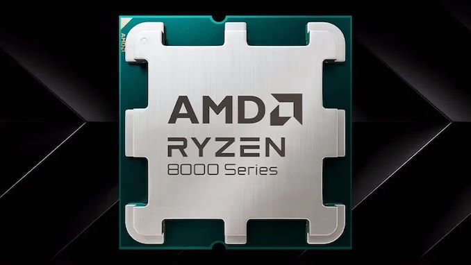
AMD has recently expanded its Ryzen 8000 series by introducing the Ryzen 7 8700F and Ryzen 5 8400F processors. Initially launched in China, these chips were added to AMD's global website, signaling they are available worldwide, apparently from April 1st. Built from the recent Zen 4-based Phoenix APUs using the TSMC 4nm node as their Zen 4 mobile chips, these new CPUs lack integrated graphics. However, the Ryzen 7 8700F does include the integrated Ryzen AI NPU for added capabilities in a world currently dominated by AI and moving it directly into the PC.
The company's decision to announce these chips in China aligns with its strategy to offer Ryzen solutions at every price point in the market. Although AMD didn't initially disclose the full specifications of these F-series models, and we did reach out to the company to ask about them, they refused to discuss them with us. Their listing on the website has now been updated with a complete list of specifications and features, with everything but the price mentioned.
| AMD Ryzen 8000G vs. Ryzen 8000F Series (Desktop) Zen 4 (Phoenix) |
|||||||||
| AnandTech | Cores/Threads | Base Freq |
Turbo Freq |
GPU | GPU Freq |
Ryzen AI (NPU) |
L3 Cache (MB) |
TDP | MSRP |
| Ryzen 7 | |||||||||
| Ryzen 7 8700G | 8/16 | 4200 | 5100 | R780M 12 CUs |
2900 | Y | 16 | 65W | $329 |
| Ryzen 7 8700F | 8/16 | 4100 | 5000 | - | - | Y | 16 | 65W | ? |
| Ryzen 5 | |||||||||
| Ryzen 5 8600G | 6/12 | 4300 | 5000 | R760M 8 CUs |
2800 | Y | 16 | 65W | $229 |
| Ryzen 5 8400F | 6/12 | 4200 | 4700 | - | - | N | 16 | 65W | ? |
The Ryzen 7 8700F features an 8C/16T design, with 16MB of L3 cache and the same 65W TDP as the Ryzen 7 8700G. Although the base clock speed is 4.1 GHz, it boosts to 5.0 GHz; this is 100 MHz less on both base/boost clocks than the 8700G. Meanwhile, the Ryzen 5 8400F is a slightly scaled-down version of the Ryzen 8600G APU, with 6C/12, 16MB of L3 cache, and again has a 100 MHz reduction to base clocks compared to the 8600G. Unlike the Ryzen 5 8400F, the Ryzen 7 8700F keeps AMD's Ryzen AI NPU, adding additional capability for generative AI.
The Ryzen 5 8400F can boost up to 4.7 GHz, 300 MHz slower than the Ryzen 5 8600G. AMD also allows overclocking for these new F-series chips, which means users could potentially boost the performance of these processors to match their G-series equivalents.
Pricing details are still pending, but to remain competitive, AMD will likely need to price these CPUs below the 8700G and 8600G, as well as the Ryzen 7 7700 and Ryzen 5 7600. These CPUs offer, albeit very limited, integrated graphics and have double the L3 cache capacity, along with higher boost clocks than the 8000F series chips, so pricing is something to consider whenever pricing becomes available.
CPUs
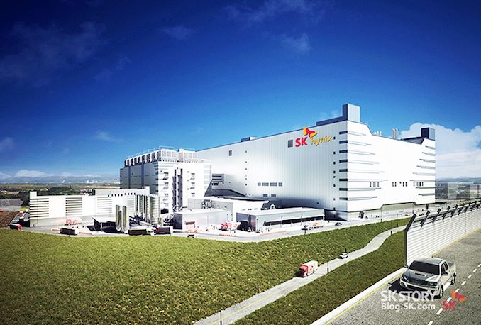
When a major industry slowdown occurs, big companies tend to slowdown their mid-term and long-term capacity related investments. This is exactly what happened to SK hynix's Yongin Semiconductor Cluster, a major project announced in April 2021 and valued at $106 billion. While development of the site has been largely completed, only 35% of the initial shell building has been constructed, according to the Korean Ministry of Trade, Industry, and Energy.
"Approximately 35% of Fab 1 has been completed so far and site renovation is in smooth progress," a statement by the Korean Ministry of Trade, Industry, and Energy reads. "By 2046, over KRW 120 trillion ($90 billion today, $106 billion in 2021) in investment will be poured to complete Fabs 1 through 4, and construction of Fab 1's production line will commence in March next year. Once completed, the infrastructure will rank as the world's largest three-story fab."
The new semiconductor fabrication cluster by SK hynix announced almost exactly three years ago is primarily meant to be used to make DRAM for PCs, mobile devices, and servers using advanced extreme ultraviolet lithography (EUV) process technologies. The cluster, located near Yongin, South Korea, is intended to consist of four large fabs situated on a 4.15 million m2 site. With a planned capacity of approximately 800,000 wafer starts per month (WSPMs), it is set to be one of the world's largest semiconductor production hubs.
With that said, SK hynix's construction progress has been slower than the company first projected. The first fab in the complex was originally meant to come online in 2025, with construction starting in the fourth quarter of 2021. However, SK hynix began to cut its capital expenditures in the second half of 2022, and the Yongin Semiconductor Cluster project fell a victim of that cut. To be sure, the site continues to be developed, just at a slower pace; which is why some 35% of the first fab shell has been built at this point.
If completed as planned in 2021, the first phase of SK hynix Yongin operations would have been a major memory production facility costing $25 billion, equipped with EUV tools, and capable of 200,000-WSPM, according to reports from 2021.
Sources: Korean Ministry of Trade, Industry, and Energy; ComputerBase
Memory
Lorem Ipsum is simply dummy text of the printing and typesetting industry. Lorem Ipsum has been the industry's.
Western Digital's BiCS8 218-layer 3D NAND is being put to good use in a wide range of client and enterprise platforms, including WD's upcoming Gen 5 client SSDs and 128 TB-class datacenter SSD. On the external storage front, the company demonstrated four different products: for card-based media, 4 TB microSDUC and 8 TB SDUC cards with UHS-I speeds, and on the portable SSD front we had two 16 TB drives. One will be a SanDisk Desk Drive with external power, and the other in the SanDisk Extreme Pro housing with a lanyard opening in the case.
All of these are using BiCS8 QLC NAND, though I did hear booth talk (as I was taking leave) that they were not supposed to divulge the use of QLC in these products. The 4 TB microSDUC and 8 TB SDUC cards are rated for UHS-I speeds. They are being marketed under the SanDisk Ultra branding.
The SanDisk Desk Drive is an external SSD with a 18W power adapter, and it has been in the market for a few months now. Initially launched in capacities up to 8 TB, Western Digital had promised a 16 TB version before the end of the year. It appears that the product is coming to retail quite soon. One aspect to note is that this drive has been using TLC for the SKUs that are currently in the market, so it appears unlikely that the 16 TB version would be QLC. The units (at least up to the 8 TB capacity point) come with two SN850XE drives. Given the recent introduction of the 8 TB SN850X, an 'E' version with tweaked firmware is likely to be present in the 16 TB Desk Drive.
The 16 TB portable SSD in the SanDisk Extreme housing was a technology demonstration. It is definitely the highest capacity bus-powered portable SSD demonstrated by any vendor at any trade show thus far. Given the 16 TB Desk Drive's imminent market introduction, it is just a matter of time before the technology demonstration of the bus-powered version becomes a retail reality.
Storage

</td>
</tr>
<tr class="tlblue">
<td align="center" valign="middle" width="137">Manufacturing Excellence</td>
<td align="center" valign="middle" width="137">Sustainability</td>
</tr>
<tr>
<td align="center" valign="middle">Global One Fab Manufacturing</td>
<td align="center" valign="middle">Green Manufacturing</td>
</tr>
<tr>
<td align="center" valign="middle">ML-based Process Control</td>
<td align="center" valign="middle">Global Talent Development</td>
</tr>
<tr>
<td align="center" valign="middle">Manufacturing Agility and Quality</td>
<td align="center" valign="middle">Supply Chain Localization</td>
</tr>
<tr>
<td align="center" valign="middle">Maximum Productivity</td>
<td align="center" valign="middle">Social Responsibility</td>
</tr>
</tbody>
</table>
<p>When it comes to improvements of process technology, there are two main mechanisms: the continuous process improvements (CPI) to improve yields, as well as statistical process control (SPC) reduce performance variations. To do so, the company has multiple internal techniques that rely on machine learning-based process control, constant quality measuring, and various productivity improving methods. With Global Gigafab manufacturing TSMC can use CPI and SPC to improve yields and performance on the global scale by sharing knowledge between different sites.</p>
<p>"When we port a technology from Taiwan to Arizona, the fab set up, the process control system, everything is actually a copy from Taiwan," said Kevin Zhang, Senior Vice President, Business Development and Overseas Operations Office, and Deputy Co-COO at TSMC.</p>
<p>TSMC yet has to start making chips at its fabs in Germany, Japan, and the United States, so it remains to be seen how fast the foundry will increase yields to Taiwanese levels at its Fab 23 (in Kumamoto, Japan) and Fab 21 (in Arizona) when they begin operations in 2024 and 2025, but with Global Gigafab Manufacturing program in place, this is likely set to happen rather sooner than later.</p>
</p> Semiconductors)
</td>
</tr>
<tr class="tlblue">
<td align="center" valign="middle" width="137">Manufacturing Excellence</td>
<td align="center" valign="middle" width="137">Sustainability</td>
</tr>
<tr>
<td align="center" valign="middle">Global One Fab Manufacturing</td>
<td align="center" valign="middle">Green Manufacturing</td>
</tr>
<tr>
<td align="center" valign="middle">ML-based Process Control</td>
<td align="center" valign="middle">Global Talent Development</td>
</tr>
<tr>
<td align="center" valign="middle">Manufacturing Agility and Quality</td>
<td align="center" valign="middle">Supply Chain Localization</td>
</tr>
<tr>
<td align="center" valign="middle">Maximum Productivity</td>
<td align="center" valign="middle">Social Responsibility</td>
</tr>
</tbody>
</table>
<p>When it comes to improvements of process technology, there are two main mechanisms: the continuous process improvements (CPI) to improve yields, as well as statistical process control (SPC) reduce performance variations. To do so, the company has multiple internal techniques that rely on machine learning-based process control, constant quality measuring, and various productivity improving methods. With Global Gigafab manufacturing TSMC can use CPI and SPC to improve yields and performance on the global scale by sharing knowledge between different sites.</p>
<p>"When we port a technology from Taiwan to Arizona, the fab set up, the process control system, everything is actually a copy from Taiwan," said Kevin Zhang, Senior Vice President, Business Development and Overseas Operations Office, and Deputy Co-COO at TSMC.</p>
<p>TSMC yet has to start making chips at its fabs in Germany, Japan, and the United States, so it remains to be seen how fast the foundry will increase yields to Taiwanese levels at its Fab 23 (in Kumamoto, Japan) and Fab 21 (in Arizona) when they begin operations in 2024 and 2025, but with Global Gigafab Manufacturing program in place, this is likely set to happen rather sooner than later.</p>
</p> Semiconductors)
</td>
</tr>
<tr class="tlblue">
<td align="center" valign="middle" width="137">Manufacturing Excellence</td>
<td align="center" valign="middle" width="137">Sustainability</td>
</tr>
<tr>
<td align="center" valign="middle">Global One Fab Manufacturing</td>
<td align="center" valign="middle">Green Manufacturing</td>
</tr>
<tr>
<td align="center" valign="middle">ML-based Process Control</td>
<td align="center" valign="middle">Global Talent Development</td>
</tr>
<tr>
<td align="center" valign="middle">Manufacturing Agility and Quality</td>
<td align="center" valign="middle">Supply Chain Localization</td>
</tr>
<tr>
<td align="center" valign="middle">Maximum Productivity</td>
<td align="center" valign="middle">Social Responsibility</td>
</tr>
</tbody>
</table>
<p>When it comes to improvements of process technology, there are two main mechanisms: the continuous process improvements (CPI) to improve yields, as well as statistical process control (SPC) reduce performance variations. To do so, the company has multiple internal techniques that rely on machine learning-based process control, constant quality measuring, and various productivity improving methods. With Global Gigafab manufacturing TSMC can use CPI and SPC to improve yields and performance on the global scale by sharing knowledge between different sites.</p>
<p>"When we port a technology from Taiwan to Arizona, the fab set up, the process control system, everything is actually a copy from Taiwan," said Kevin Zhang, Senior Vice President, Business Development and Overseas Operations Office, and Deputy Co-COO at TSMC.</p>
<p>TSMC yet has to start making chips at its fabs in Germany, Japan, and the United States, so it remains to be seen how fast the foundry will increase yields to Taiwanese levels at its Fab 23 (in Kumamoto, Japan) and Fab 21 (in Arizona) when they begin operations in 2024 and 2025, but with Global Gigafab Manufacturing program in place, this is likely set to happen rather sooner than later.</p>
</p> Semiconductors | https://compbuddey.blogspot.com/2024/05/tsmc-offers-peek-at-global-gigafab_30.html)
</td>
</tr>
<tr class="tlblue">
<td align="center" valign="middle" width="137">Manufacturing Excellence</td>
<td align="center" valign="middle" width="137">Sustainability</td>
</tr>
<tr>
<td align="center" valign="middle">Global One Fab Manufacturing</td>
<td align="center" valign="middle">Green Manufacturing</td>
</tr>
<tr>
<td align="center" valign="middle">ML-based Process Control</td>
<td align="center" valign="middle">Global Talent Development</td>
</tr>
<tr>
<td align="center" valign="middle">Manufacturing Agility and Quality</td>
<td align="center" valign="middle">Supply Chain Localization</td>
</tr>
<tr>
<td align="center" valign="middle">Maximum Productivity</td>
<td align="center" valign="middle">Social Responsibility</td>
</tr>
</tbody>
</table>
<p>When it comes to improvements of process technology, there are two main mechanisms: the continuous process improvements (CPI) to improve yields, as well as statistical process control (SPC) reduce performance variations. To do so, the company has multiple internal techniques that rely on machine learning-based process control, constant quality measuring, and various productivity improving methods. With Global Gigafab manufacturing TSMC can use CPI and SPC to improve yields and performance on the global scale by sharing knowledge between different sites.</p>
<p>"When we port a technology from Taiwan to Arizona, the fab set up, the process control system, everything is actually a copy from Taiwan," said Kevin Zhang, Senior Vice President, Business Development and Overseas Operations Office, and Deputy Co-COO at TSMC.</p>
<p>TSMC yet has to start making chips at its fabs in Germany, Japan, and the United States, so it remains to be seen how fast the foundry will increase yields to Taiwanese levels at its Fab 23 (in Kumamoto, Japan) and Fab 21 (in Arizona) when they begin operations in 2024 and 2025, but with Global Gigafab Manufacturing program in place, this is likely set to happen rather sooner than later.</p>
</p> Semiconductors&body=https://compbuddey.blogspot.com/2024/05/tsmc-offers-peek-at-global-gigafab_30.html)


0 Comments