

Optical connectivity – and especially silicon photonics – is expected to become a crucial technology to enable connectivity for next-generation datacenters, particularly those designed HPC applications. With ever-increasing bandwidth requirements needed to keep up with (and keep scaling out) system performance, copper signaling alone won't be enough to keep up. To that end, several companies are developing silicon photonics solutions, including fab providers like TSMC, who this week outlined its 3D Optical Engine roadmap as part of its 2024 North American Technology Symposium, laying out its plan to bring up to 12.8 Tbps optical connectivity to TSMC-fabbed processors.
TSMC's Compact Universal Photonic Engine (COUPE) stacks an electronics integrated circuit on photonic integrated circuit (EIC-on-PIC) using the company's SoIC-X packaging technology. The foundry says that usage of its SoIC-X enables the lowest impedance at the die-to-die interface and therefore the highest energy efficiency. The EIC itself is produced at a 65nm-class process technology.
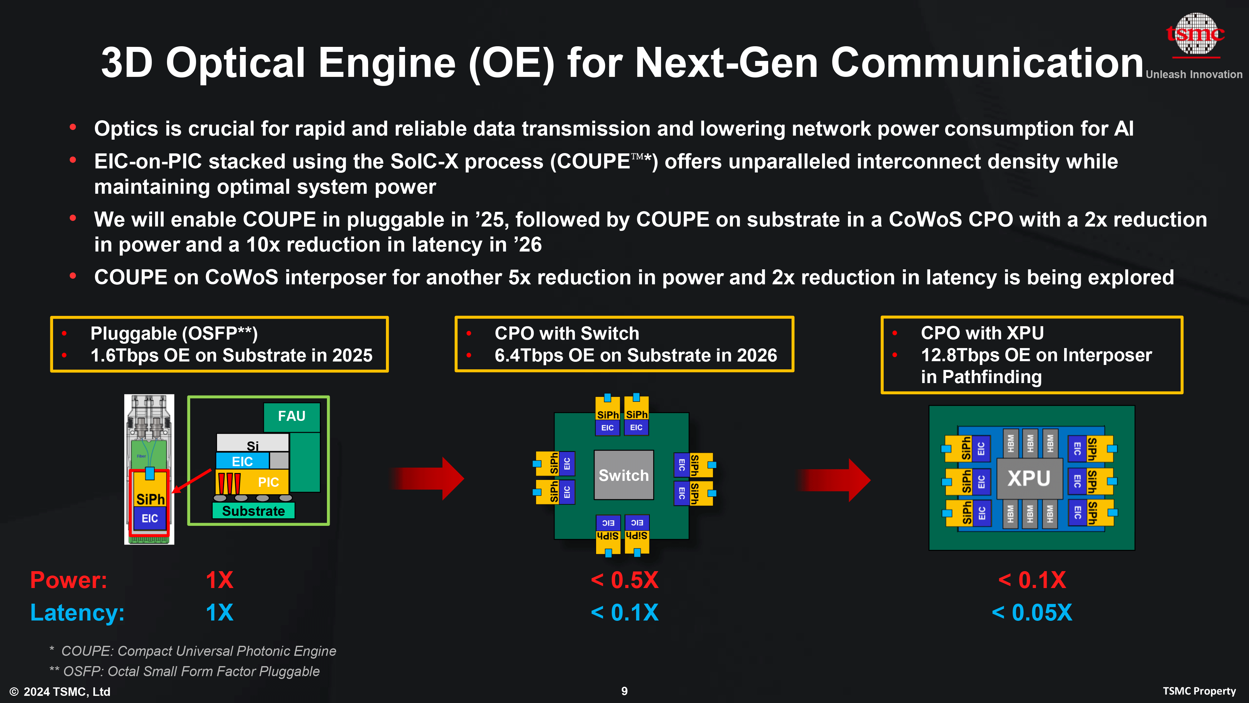
TSMC's 1st Generation 3D Optical Engine (or COUPE) will be integrated into an OSFP pluggable device running at 1.6 Tbps. That's a transfer rate well ahead of current copper Ethernet standards – which top out at 800 Gbps – underscoring the immediate bandwidth advantage of optical interconnects for heavily-networked compute clusters, never mind the expected power savings.
Looking further ahead, the 2nd Generation of COUPE is designed to integrate into CoWoS packaging as co-packaged optics with a switch, allowing optical interconnections to be brought to the motherboard level. This version COUPE will support data transfer rates of up to 6.40 Tbps with reduced latency compared to the first version.
TSMC's third iteration of COUPE – COUPE running on a CoWoS interposer – is projected to improve on things one step further, increasing transfer rates to 12.8 Tbps while bringing optical connectivity even closer to the processor itself. At present, COUPE-on-CoWoS is in the pathfinding stage of development and TSMC does not have a target date set.
Ultimately, unlike many of its industry peers, TSMC has not participated in the silicon photonics market up until now, leaving this to players like GlobalFoundries. But with its 3D Optical Engine Strategy, the company will enter this important market as it looks to make up for lost time.


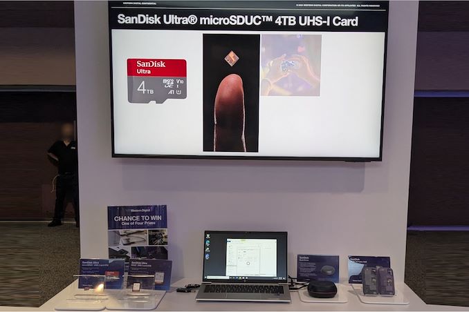
Western Digital's BiCS8 218-layer 3D NAND is being put to good use in a wide range of client and enterprise platforms, including WD's upcoming Gen 5 client SSDs and 128 TB-class datacenter SSD. On the external storage front, the company demonstrated four different products: for card-based media, 4 TB microSDUC and 8 TB SDUC cards with UHS-I speeds, and on the portable SSD front we had two 16 TB drives. One will be a SanDisk Desk Drive with external power, and the other in the SanDisk Extreme Pro housing with a lanyard opening in the case.
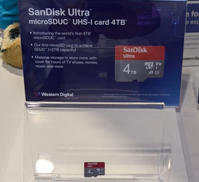
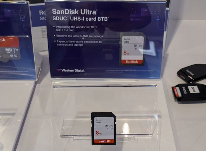
All of these are using BiCS8 QLC NAND, though I did hear booth talk (as I was taking leave) that they were not supposed to divulge the use of QLC in these products. The 4 TB microSDUC and 8 TB SDUC cards are rated for UHS-I speeds. They are being marketed under the SanDisk Ultra branding.
The SanDisk Desk Drive is an external SSD with a 18W power adapter, and it has been in the market for a few months now. Initially launched in capacities up to 8 TB, Western Digital had promised a 16 TB version before the end of the year. It appears that the product is coming to retail quite soon. One aspect to note is that this drive has been using TLC for the SKUs that are currently in the market, so it appears unlikely that the 16 TB version would be QLC. The units (at least up to the 8 TB capacity point) come with two SN850XE drives. Given the recent introduction of the 8 TB SN850X, an 'E' version with tweaked firmware is likely to be present in the 16 TB Desk Drive.
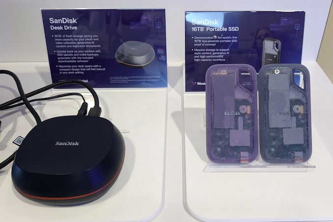
The 16 TB portable SSD in the SanDisk Extreme housing was a technology demonstration. It is definitely the highest capacity bus-powered portable SSD demonstrated by any vendor at any trade show thus far. Given the 16 TB Desk Drive's imminent market introduction, it is just a matter of time before the technology demonstration of the bus-powered version becomes a retail reality.
Storage
Western Digital's BiCS8 218-layer 3D NAND is being put to good use in a wide range of client and enterprise platforms, including WD's upcoming Gen 5 client SSDs and 128 TB-class datacenter SSD. On the external storage front, the company demonstrated four different products: for card-based media, 4 TB microSDUC and 8 TB SDUC cards with UHS-I speeds, and on the portable SSD front we had two 16 TB drives. One will be a SanDisk Desk Drive with external power, and the other in the SanDisk Extreme Pro housing with a lanyard opening in the case.
All of these are using BiCS8 QLC NAND, though I did hear booth talk (as I was taking leave) that they were not supposed to divulge the use of QLC in these products. The 4 TB microSDUC and 8 TB SDUC cards are rated for UHS-I speeds. They are being marketed under the SanDisk Ultra branding.
The SanDisk Desk Drive is an external SSD with a 18W power adapter, and it has been in the market for a few months now. Initially launched in capacities up to 8 TB, Western Digital had promised a 16 TB version before the end of the year. It appears that the product is coming to retail quite soon. One aspect to note is that this drive has been using TLC for the SKUs that are currently in the market, so it appears unlikely that the 16 TB version would be QLC. The units (at least up to the 8 TB capacity point) come with two SN850XE drives. Given the recent introduction of the 8 TB SN850X, an 'E' version with tweaked firmware is likely to be present in the 16 TB Desk Drive.
The 16 TB portable SSD in the SanDisk Extreme housing was a technology demonstration. It is definitely the highest capacity bus-powered portable SSD demonstrated by any vendor at any trade show thus far. Given the 16 TB Desk Drive's imminent market introduction, it is just a matter of time before the technology demonstration of the bus-powered version becomes a retail reality.
Storage
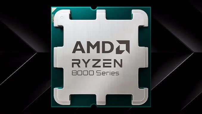
AMD has recently expanded its Ryzen 8000 series by introducing the Ryzen 7 8700F and Ryzen 5 8400F processors. Initially launched in China, these chips were added to AMD's global website, signaling they are available worldwide, apparently from April 1st. Built from the recent Zen 4-based Phoenix APUs using the TSMC 4nm node as their Zen 4 mobile chips, these new CPUs lack integrated graphics. However, the Ryzen 7 8700F does include the integrated Ryzen AI NPU for added capabilities in a world currently dominated by AI and moving it directly into the PC.
The company's decision to announce these chips in China aligns with its strategy to offer Ryzen solutions at every price point in the market. Although AMD didn't initially disclose the full specifications of these F-series models, and we did reach out to the company to ask about them, they refused to discuss them with us. Their listing on the website has now been updated with a complete list of specifications and features, with everything but the price mentioned.
| AMD Ryzen 8000G vs. Ryzen 8000F Series (Desktop) Zen 4 (Phoenix) |
|||||||||
| AnandTech | Cores/Threads | Base Freq |
Turbo Freq |
GPU | GPU Freq |
Ryzen AI (NPU) |
L3 Cache (MB) |
TDP | MSRP |
| Ryzen 7 | |||||||||
| Ryzen 7 8700G | 8/16 | 4200 | 5100 | R780M 12 CUs |
2900 | Y | 16 | 65W | $329 |
| Ryzen 7 8700F | 8/16 | 4100 | 5000 | - | - | Y | 16 | 65W | ? |
| Ryzen 5 | |||||||||
| Ryzen 5 8600G | 6/12 | 4300 | 5000 | R760M 8 CUs |
2800 | Y | 16 | 65W | $229 |
| Ryzen 5 8400F | 6/12 | 4200 | 4700 | - | - | N | 16 | 65W | ? |
The Ryzen 7 8700F features an 8C/16T design, with 16MB of L3 cache and the same 65W TDP as the Ryzen 7 8700G. Although the base clock speed is 4.1 GHz, it boosts to 5.0 GHz; this is 100 MHz less on both base/boost clocks than the 8700G. Meanwhile, the Ryzen 5 8400F is a slightly scaled-down version of the Ryzen 8600G APU, with 6C/12, 16MB of L3 cache, and again has a 100 MHz reduction to base clocks compared to the 8600G. Unlike the Ryzen 5 8400F, the Ryzen 7 8700F keeps AMD's Ryzen AI NPU, adding additional capability for generative AI.
The Ryzen 5 8400F can boost up to 4.7 GHz, 300 MHz slower than the Ryzen 5 8600G. AMD also allows overclocking for these new F-series chips, which means users could potentially boost the performance of these processors to match their G-series equivalents.
Pricing details are still pending, but to remain competitive, AMD will likely need to price these CPUs below the 8700G and 8600G, as well as the Ryzen 7 7700 and Ryzen 5 7600. These CPUs offer, albeit very limited, integrated graphics and have double the L3 cache capacity, along with higher boost clocks than the 8000F series chips, so pricing is something to consider whenever pricing becomes available.
CPUs
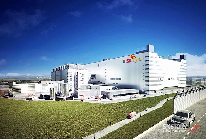
When a major industry slowdown occurs, big companies tend to slowdown their mid-term and long-term capacity related investments. This is exactly what happened to SK hynix's Yongin Semiconductor Cluster, a major project announced in April 2021 and valued at $106 billion. While development of the site has been largely completed, only 35% of the initial shell building has been constructed, according to the Korean Ministry of Trade, Industry, and Energy.
"Approximately 35% of Fab 1 has been completed so far and site renovation is in smooth progress," a statement by the Korean Ministry of Trade, Industry, and Energy reads. "By 2046, over KRW 120 trillion ($90 billion today, $106 billion in 2021) in investment will be poured to complete Fabs 1 through 4, and construction of Fab 1's production line will commence in March next year. Once completed, the infrastructure will rank as the world's largest three-story fab."
The new semiconductor fabrication cluster by SK hynix announced almost exactly three years ago is primarily meant to be used to make DRAM for PCs, mobile devices, and servers using advanced extreme ultraviolet lithography (EUV) process technologies. The cluster, located near Yongin, South Korea, is intended to consist of four large fabs situated on a 4.15 million m2 site. With a planned capacity of approximately 800,000 wafer starts per month (WSPMs), it is set to be one of the world's largest semiconductor production hubs.
With that said, SK hynix's construction progress has been slower than the company first projected. The first fab in the complex was originally meant to come online in 2025, with construction starting in the fourth quarter of 2021. However, SK hynix began to cut its capital expenditures in the second half of 2022, and the Yongin Semiconductor Cluster project fell a victim of that cut. To be sure, the site continues to be developed, just at a slower pace; which is why some 35% of the first fab shell has been built at this point.
If completed as planned in 2021, the first phase of SK hynix Yongin operations would have been a major memory production facility costing $25 billion, equipped with EUV tools, and capable of 200,000-WSPM, according to reports from 2021.
Sources: Korean Ministry of Trade, Industry, and Energy; ComputerBase
Memory
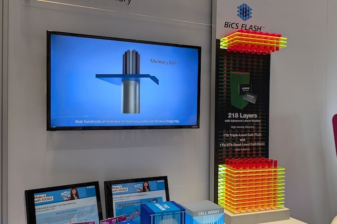
Kioxia's booth at FMS 2024 was a busy one with multiple technology demonstrations keeping visitors occupied. A walk-through of the BiCS 8 manufacturing process was the first to grab my attention. Kioxia and Western Digital announced the sampling of BiCS 8 in March 2023. We had touched briefly upon its CMOS Bonded Array (CBA) scheme in our coverage of Kioxial's 2Tb QLC NAND device and coverage of Western Digital's 128 TB QLC enterprise SSD proof-of-concept demonstration. At Kioxia's booth, we got more insights.
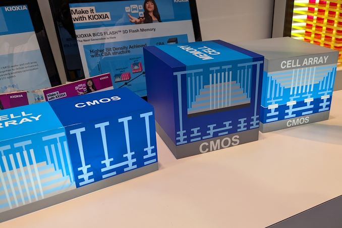
Traditionally, fabrication of flash chips involved placement of the associate logic circuitry (CMOS process) around the periphery of the flash array. The process then moved on to putting the CMOS under the cell array, but the wafer development process was serialized with the CMOS logic getting fabricated first followed by the cell array on top. However, this has some challenges because the cell array requires a high-temperature processing step to ensure higher reliability that can be detrimental to the health of the CMOS logic. Thanks to recent advancements in wafer bonding techniques, the new CBA process allows the CMOS wafer and cell array wafer to be processed independently in parallel and then pieced together, as shown in the models above.
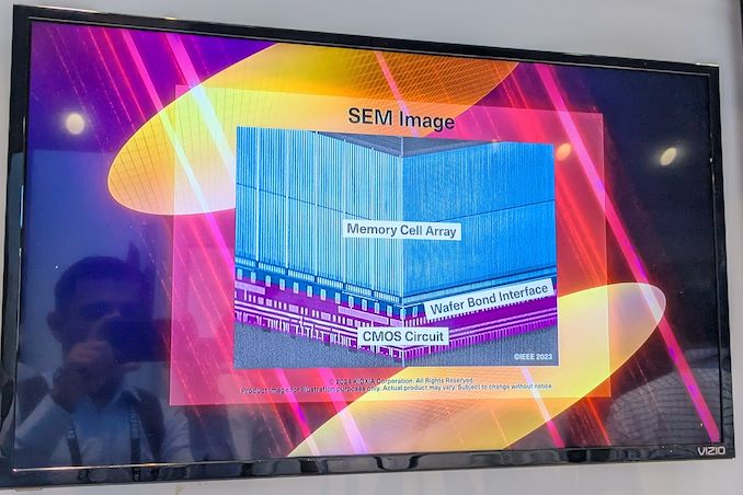
The BiCS 8 3D NAND incorporates 218 layers, compared to 112 layers in BiCS 5 and 162 layers in BiCS 6. The company decided to skip over BiCS 7 (or, rather, it was probably a short-lived generation meant as an internal test vehicle). The generation retains the four-plane charge trap structure of BiCS 6. In its TLC avatar, it is available as a 1 Tbit device. The QLC version is available in two capacities - 1 Tbit and 2 Tbit.
Kioxia also noted that while the number of layers (218) doesn't compare favorably with the latest layer counts from the competition, its lateral scaling / cell shrinkage has enabled it to be competitive in terms of bit density as well as operating speeds (3200 MT/s). For reference, the latest shipping NAND from Micron - the G9 - has 276 layers with a bit density in TLC mode of 21 Gbit/mm2, and operates at up to 3600 MT/s. However, its 232L NAND operates only up to 2400 MT/s and has a bit density of 14.6 Gbit/mm2.
It must be noted that the CBA hybrid bonding process has advantages over the current processes used by other vendors - including Micron's CMOS under array (CuA) and SK hynix's 4D PUC (periphery-under-chip) developed in the late 2010s. It is expected that other NAND vendors will also move eventually to some variant of the hybrid bonding scheme used by Kioxia.
Storage
Lorem Ipsum is simply dummy text of the printing and typesetting industry. Lorem Ipsum has been the industry's.
Western Digital's BiCS8 218-layer 3D NAND is being put to good use in a wide range of client and enterprise platforms, including WD's upcoming Gen 5 client SSDs and 128 TB-class datacenter SSD. On the external storage front, the company demonstrated four different products: for card-based media, 4 TB microSDUC and 8 TB SDUC cards with UHS-I speeds, and on the portable SSD front we had two 16 TB drives. One will be a SanDisk Desk Drive with external power, and the other in the SanDisk Extreme Pro housing with a lanyard opening in the case.
All of these are using BiCS8 QLC NAND, though I did hear booth talk (as I was taking leave) that they were not supposed to divulge the use of QLC in these products. The 4 TB microSDUC and 8 TB SDUC cards are rated for UHS-I speeds. They are being marketed under the SanDisk Ultra branding.
The SanDisk Desk Drive is an external SSD with a 18W power adapter, and it has been in the market for a few months now. Initially launched in capacities up to 8 TB, Western Digital had promised a 16 TB version before the end of the year. It appears that the product is coming to retail quite soon. One aspect to note is that this drive has been using TLC for the SKUs that are currently in the market, so it appears unlikely that the 16 TB version would be QLC. The units (at least up to the 8 TB capacity point) come with two SN850XE drives. Given the recent introduction of the 8 TB SN850X, an 'E' version with tweaked firmware is likely to be present in the 16 TB Desk Drive.
The 16 TB portable SSD in the SanDisk Extreme housing was a technology demonstration. It is definitely the highest capacity bus-powered portable SSD demonstrated by any vendor at any trade show thus far. Given the 16 TB Desk Drive's imminent market introduction, it is just a matter of time before the technology demonstration of the bus-powered version becomes a retail reality.
Storage

 system performance, copper signaling alone won't be enough to keep up. To that end, several companies are developing silicon photonics solutions, including fab providers like TSMC, who this week outlined its 3D Optical Engine roadmap as part of its 2024 North American Technology Symposium, laying out its plan to bring up to 12.8 Tbps optical connectivity to TSMC-fabbed processors.</p>
<p>TSMC's Compact Universal Photonic Engine (COUPE) stacks an electronics integrated circuit on photonic integrated circuit (EIC-on-PIC) using the company's SoIC-X packaging technology. The foundry says that usage of its SoIC-X enables the lowest impedance at the die-to-die interface and therefore the highest energy efficiency. The EIC itself is produced at a 65nm-class process technology.</p>
<p style="text-align: center;"><a href="https://www.anandtech.com/show/21373/tsmc-adds-silicon-photonics-coupe-roadmap-128tbps-on-package"><img alt="" src="https://images.anandtech.com/doci/21373/TSMC-3D-Optical-Engine.png" style="width: 100%;" /></a></p>
<p>TSMC's 1st Generation 3D Optical Engine (or COUPE) will be integrated into an OSFP pluggable device running at 1.6 Tbps. That's a transfer rate well ahead of current copper Ethernet standards – which top out at 800 Gbps – underscoring the immediate bandwidth advantage of optical interconnects for heavily-networked compute clusters, never mind the expected power savings.</p>
<p>Looking further ahead, the 2nd Generation of COUPE is designed to integrate into CoWoS packaging as co-packaged optics with a switch, allowing optical interconnections to be brought to the motherboard level. This version COUPE will support data transfer rates of up to 6.40 Tbps with reduced latency compared to the first version.</p>
<p>TSMC's third iteration of COUPE – COUPE running on a CoWoS interposer – is projected to improve on things one step further, increasing transfer rates to 12.8 Tbps while bringing optical connectivity even closer to the processor itself. At present, COUPE-on-CoWoS is in the pathfinding stage of development and TSMC does not have a target date set.</p>
<p>Ultimately, unlike many of its industry peers, TSMC has not participated in the silicon photonics market up until now, leaving this to players like GlobalFoundries. But with its 3D Optical Engine Strategy, the company will enter this important market as it looks to make up for lost time.</p>
<h3><strong>Related Reading</strong></h3>
<ul>
<li><a href="https://www.anandtech.com/show/21369/tsmcs-16nm-technology-announced-for-late-2026-a16-with-super-power-rail-bspdn">TSMC's 1.6nm Technology Announced for Late 2026: A16 with "Super Power Rail" Backside Power</a></li>
<li><a href="https://www.anandtech.com/show/21370/tsmc-2nm-update-n2-in-2025-n2p-loses-bspdn-nanoflex-optimizations">TSMC 2nm Update: N2 In 2025, N2P Loses Backside Power, and NanoFlex Brings Optimal Cells</a></li>
<li><a href="https://www.anandtech.com/show/21371/tsmc-preps-lower-cost-4nm-n4c-process-for-2025">TSMC Preps Cheaper 4nm N4C Process For 2025, Aiming For 8.5% Cost Reduction</a></li>
<li><a href="https://www.anandtech.com/show/21372/tsmcs-system-on-wafer-platform-goes-3d-cow-sow">TSMC's System-on-Wafer Platform Goes 3D: CoW-SoW Stacks Up the Chips</a></li>
</ul>
</p> Semiconductors)
 system performance, copper signaling alone won't be enough to keep up. To that end, several companies are developing silicon photonics solutions, including fab providers like TSMC, who this week outlined its 3D Optical Engine roadmap as part of its 2024 North American Technology Symposium, laying out its plan to bring up to 12.8 Tbps optical connectivity to TSMC-fabbed processors.</p>
<p>TSMC's Compact Universal Photonic Engine (COUPE) stacks an electronics integrated circuit on photonic integrated circuit (EIC-on-PIC) using the company's SoIC-X packaging technology. The foundry says that usage of its SoIC-X enables the lowest impedance at the die-to-die interface and therefore the highest energy efficiency. The EIC itself is produced at a 65nm-class process technology.</p>
<p style="text-align: center;"><a href="https://www.anandtech.com/show/21373/tsmc-adds-silicon-photonics-coupe-roadmap-128tbps-on-package"><img alt="" src="https://images.anandtech.com/doci/21373/TSMC-3D-Optical-Engine.png" style="width: 100%;" /></a></p>
<p>TSMC's 1st Generation 3D Optical Engine (or COUPE) will be integrated into an OSFP pluggable device running at 1.6 Tbps. That's a transfer rate well ahead of current copper Ethernet standards – which top out at 800 Gbps – underscoring the immediate bandwidth advantage of optical interconnects for heavily-networked compute clusters, never mind the expected power savings.</p>
<p>Looking further ahead, the 2nd Generation of COUPE is designed to integrate into CoWoS packaging as co-packaged optics with a switch, allowing optical interconnections to be brought to the motherboard level. This version COUPE will support data transfer rates of up to 6.40 Tbps with reduced latency compared to the first version.</p>
<p>TSMC's third iteration of COUPE – COUPE running on a CoWoS interposer – is projected to improve on things one step further, increasing transfer rates to 12.8 Tbps while bringing optical connectivity even closer to the processor itself. At present, COUPE-on-CoWoS is in the pathfinding stage of development and TSMC does not have a target date set.</p>
<p>Ultimately, unlike many of its industry peers, TSMC has not participated in the silicon photonics market up until now, leaving this to players like GlobalFoundries. But with its 3D Optical Engine Strategy, the company will enter this important market as it looks to make up for lost time.</p>
<h3><strong>Related Reading</strong></h3>
<ul>
<li><a href="https://www.anandtech.com/show/21369/tsmcs-16nm-technology-announced-for-late-2026-a16-with-super-power-rail-bspdn">TSMC's 1.6nm Technology Announced for Late 2026: A16 with "Super Power Rail" Backside Power</a></li>
<li><a href="https://www.anandtech.com/show/21370/tsmc-2nm-update-n2-in-2025-n2p-loses-bspdn-nanoflex-optimizations">TSMC 2nm Update: N2 In 2025, N2P Loses Backside Power, and NanoFlex Brings Optimal Cells</a></li>
<li><a href="https://www.anandtech.com/show/21371/tsmc-preps-lower-cost-4nm-n4c-process-for-2025">TSMC Preps Cheaper 4nm N4C Process For 2025, Aiming For 8.5% Cost Reduction</a></li>
<li><a href="https://www.anandtech.com/show/21372/tsmcs-system-on-wafer-platform-goes-3d-cow-sow">TSMC's System-on-Wafer Platform Goes 3D: CoW-SoW Stacks Up the Chips</a></li>
</ul>
</p> Semiconductors)
 system performance, copper signaling alone won't be enough to keep up. To that end, several companies are developing silicon photonics solutions, including fab providers like TSMC, who this week outlined its 3D Optical Engine roadmap as part of its 2024 North American Technology Symposium, laying out its plan to bring up to 12.8 Tbps optical connectivity to TSMC-fabbed processors.</p>
<p>TSMC's Compact Universal Photonic Engine (COUPE) stacks an electronics integrated circuit on photonic integrated circuit (EIC-on-PIC) using the company's SoIC-X packaging technology. The foundry says that usage of its SoIC-X enables the lowest impedance at the die-to-die interface and therefore the highest energy efficiency. The EIC itself is produced at a 65nm-class process technology.</p>
<p style="text-align: center;"><a href="https://www.anandtech.com/show/21373/tsmc-adds-silicon-photonics-coupe-roadmap-128tbps-on-package"><img alt="" src="https://images.anandtech.com/doci/21373/TSMC-3D-Optical-Engine.png" style="width: 100%;" /></a></p>
<p>TSMC's 1st Generation 3D Optical Engine (or COUPE) will be integrated into an OSFP pluggable device running at 1.6 Tbps. That's a transfer rate well ahead of current copper Ethernet standards – which top out at 800 Gbps – underscoring the immediate bandwidth advantage of optical interconnects for heavily-networked compute clusters, never mind the expected power savings.</p>
<p>Looking further ahead, the 2nd Generation of COUPE is designed to integrate into CoWoS packaging as co-packaged optics with a switch, allowing optical interconnections to be brought to the motherboard level. This version COUPE will support data transfer rates of up to 6.40 Tbps with reduced latency compared to the first version.</p>
<p>TSMC's third iteration of COUPE – COUPE running on a CoWoS interposer – is projected to improve on things one step further, increasing transfer rates to 12.8 Tbps while bringing optical connectivity even closer to the processor itself. At present, COUPE-on-CoWoS is in the pathfinding stage of development and TSMC does not have a target date set.</p>
<p>Ultimately, unlike many of its industry peers, TSMC has not participated in the silicon photonics market up until now, leaving this to players like GlobalFoundries. But with its 3D Optical Engine Strategy, the company will enter this important market as it looks to make up for lost time.</p>
<h3><strong>Related Reading</strong></h3>
<ul>
<li><a href="https://www.anandtech.com/show/21369/tsmcs-16nm-technology-announced-for-late-2026-a16-with-super-power-rail-bspdn">TSMC's 1.6nm Technology Announced for Late 2026: A16 with "Super Power Rail" Backside Power</a></li>
<li><a href="https://www.anandtech.com/show/21370/tsmc-2nm-update-n2-in-2025-n2p-loses-bspdn-nanoflex-optimizations">TSMC 2nm Update: N2 In 2025, N2P Loses Backside Power, and NanoFlex Brings Optimal Cells</a></li>
<li><a href="https://www.anandtech.com/show/21371/tsmc-preps-lower-cost-4nm-n4c-process-for-2025">TSMC Preps Cheaper 4nm N4C Process For 2025, Aiming For 8.5% Cost Reduction</a></li>
<li><a href="https://www.anandtech.com/show/21372/tsmcs-system-on-wafer-platform-goes-3d-cow-sow">TSMC's System-on-Wafer Platform Goes 3D: CoW-SoW Stacks Up the Chips</a></li>
</ul>
</p> Semiconductors | https://compbuddey.blogspot.com/2024/05/tsmc-jumps-into-silicon-photonics-lays_83.html)
 system performance, copper signaling alone won't be enough to keep up. To that end, several companies are developing silicon photonics solutions, including fab providers like TSMC, who this week outlined its 3D Optical Engine roadmap as part of its 2024 North American Technology Symposium, laying out its plan to bring up to 12.8 Tbps optical connectivity to TSMC-fabbed processors.</p>
<p>TSMC's Compact Universal Photonic Engine (COUPE) stacks an electronics integrated circuit on photonic integrated circuit (EIC-on-PIC) using the company's SoIC-X packaging technology. The foundry says that usage of its SoIC-X enables the lowest impedance at the die-to-die interface and therefore the highest energy efficiency. The EIC itself is produced at a 65nm-class process technology.</p>
<p style="text-align: center;"><a href="https://www.anandtech.com/show/21373/tsmc-adds-silicon-photonics-coupe-roadmap-128tbps-on-package"><img alt="" src="https://images.anandtech.com/doci/21373/TSMC-3D-Optical-Engine.png" style="width: 100%;" /></a></p>
<p>TSMC's 1st Generation 3D Optical Engine (or COUPE) will be integrated into an OSFP pluggable device running at 1.6 Tbps. That's a transfer rate well ahead of current copper Ethernet standards – which top out at 800 Gbps – underscoring the immediate bandwidth advantage of optical interconnects for heavily-networked compute clusters, never mind the expected power savings.</p>
<p>Looking further ahead, the 2nd Generation of COUPE is designed to integrate into CoWoS packaging as co-packaged optics with a switch, allowing optical interconnections to be brought to the motherboard level. This version COUPE will support data transfer rates of up to 6.40 Tbps with reduced latency compared to the first version.</p>
<p>TSMC's third iteration of COUPE – COUPE running on a CoWoS interposer – is projected to improve on things one step further, increasing transfer rates to 12.8 Tbps while bringing optical connectivity even closer to the processor itself. At present, COUPE-on-CoWoS is in the pathfinding stage of development and TSMC does not have a target date set.</p>
<p>Ultimately, unlike many of its industry peers, TSMC has not participated in the silicon photonics market up until now, leaving this to players like GlobalFoundries. But with its 3D Optical Engine Strategy, the company will enter this important market as it looks to make up for lost time.</p>
<h3><strong>Related Reading</strong></h3>
<ul>
<li><a href="https://www.anandtech.com/show/21369/tsmcs-16nm-technology-announced-for-late-2026-a16-with-super-power-rail-bspdn">TSMC's 1.6nm Technology Announced for Late 2026: A16 with "Super Power Rail" Backside Power</a></li>
<li><a href="https://www.anandtech.com/show/21370/tsmc-2nm-update-n2-in-2025-n2p-loses-bspdn-nanoflex-optimizations">TSMC 2nm Update: N2 In 2025, N2P Loses Backside Power, and NanoFlex Brings Optimal Cells</a></li>
<li><a href="https://www.anandtech.com/show/21371/tsmc-preps-lower-cost-4nm-n4c-process-for-2025">TSMC Preps Cheaper 4nm N4C Process For 2025, Aiming For 8.5% Cost Reduction</a></li>
<li><a href="https://www.anandtech.com/show/21372/tsmcs-system-on-wafer-platform-goes-3d-cow-sow">TSMC's System-on-Wafer Platform Goes 3D: CoW-SoW Stacks Up the Chips</a></li>
</ul>
</p> Semiconductors&body=https://compbuddey.blogspot.com/2024/05/tsmc-jumps-into-silicon-photonics-lays_83.html)


0 Comments