

Optical connectivity – and especially silicon photonics – is expected to become a crucial technology to enable connectivity for next-generation datacenters, particularly those designed HPC applications. With ever-increasing bandwidth requirements needed to keep up with (and keep scaling out) system performance, copper signaling alone won't be enough to keep up. To that end, several companies are developing silicon photonics solutions, including fab providers like TSMC, who this week outlined its 3D Optical Engine roadmap as part of its 2024 North American Technology Symposium, laying out its plan to bring up to 12.8 Tbps optical connectivity to TSMC-fabbed processors.
TSMC's Compact Universal Photonic Engine (COUPE) stacks an electronics integrated circuit on photonic integrated circuit (EIC-on-PIC) using the company's SoIC-X packaging technology. The foundry says that usage of its SoIC-X enables the lowest impedance at the die-to-die interface and therefore the highest energy efficiency. The EIC itself is produced at a 65nm-class process technology.
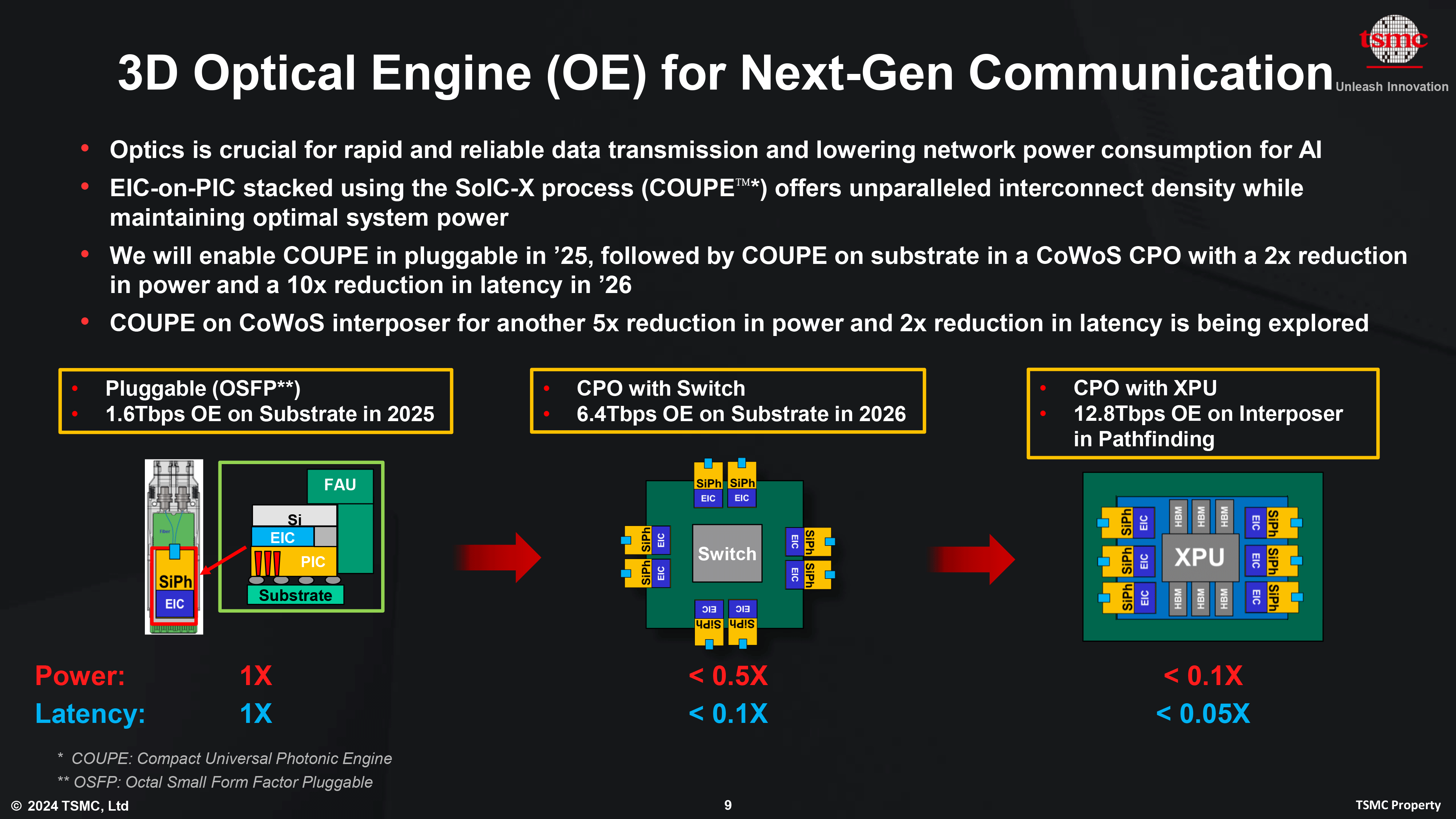
TSMC's 1st Generation 3D Optical Engine (or COUPE) will be integrated into an OSFP pluggable device running at 1.6 Tbps. That's a transfer rate well ahead of current copper Ethernet standards – which top out at 800 Gbps – underscoring the immediate bandwidth advantage of optical interconnects for heavily-networked compute clusters, never mind the expected power savings.
Looking further ahead, the 2nd Generation of COUPE is designed to integrate into CoWoS packaging as co-packaged optics with a switch, allowing optical interconnections to be brought to the motherboard level. This version COUPE will support data transfer rates of up to 6.40 Tbps with reduced latency compared to the first version.
TSMC's third iteration of COUPE – COUPE running on a CoWoS interposer – is projected to improve on things one step further, increasing transfer rates to 12.8 Tbps while bringing optical connectivity even closer to the processor itself. At present, COUPE-on-CoWoS is in the pathfinding stage of development and TSMC does not have a target date set.
Ultimately, unlike many of its industry peers, TSMC has not participated in the silicon photonics market up until now, leaving this to players like GlobalFoundries. But with its 3D Optical Engine Strategy, the company will enter this important market as it looks to make up for lost time.


Demand for high-performance processors for AI training is skyrocketing, and consequently so is the demand for the components that go into these processors. So much so that SK hynix this week is very publicly announcing that the company's high-bandwidth memory (HBM) production capacity has already sold out for the rest of 2024, and even most of 2025 has already sold out as well.
SK hynix currently produces various types of HBM memory for customers like Amazon, AMD, Facebook, Google (Broadcom), Intel, Microsoft, and, of course, NVIDIA. The latter is an especially prolific consumer of HBM3 and HBM3E memory for its H100/H200/GH200 accelerators, as NVIDIA is also working to fill what remains an insatiable (and unmet) demand for its accelerators.
As a result, HBM memory orders, which are already placed months in advance, are now backlogging well into 2025 as chip vendors look to secure supplies of the memory stacks critical to their success.
This has made SK hynix the secnd HBM memory vendor in recent months to announce that they've sold out into 2025, following an earlier announcement from Micron regarding its HBM3E production. But of the two announcements, SK hynix's is arguably the most significant yet, as the South Korean firm's HBM production capacity is far greater than Micron's. So while things were merely "interesting" with the smallest of the Big Three memory manufacturers being sold out into 2025, things are taking a more concerning (and constrained) outlook now that SK hynix is as well.
SK hynix currently controls roughly 46% - 49% of HBM market, and its share is not expected to drop significantly in 2025, according to market tracking firm TrendForce. By contrast, Micron's share on HBM memory market is between 4% and 6%. Since HBM supply of both companies is sold out through the most of 2025, we're likely looking at a scenario where over 50% of the industry's total HBM3/HBM3E supply for the coming quarters is already sold out.
This leaves Samsung as the only member of the group not to comment on HBM demand so far. Though with memory being a highly fungible commodity product, it would be surprising if Samsung wasn't facing similar demand. And, ultimately, all of this is pointing towards the indusry entering an HBM3 memory shortage.
Separately, SK hynix said that it is sampling 12-Hi 36GB HBM3E stacks with customers and will begin volume shipments in the third quarter.
Memory
Lorem Ipsum is simply dummy text of the printing and typesetting industry. Lorem Ipsum has been the industry's.
Demand for high-performance processors for AI training is skyrocketing, and consequently so is the demand for the components that go into these processors. So much so that SK hynix this week is very publicly announcing that the company's high-bandwidth memory (HBM) production capacity has already sold out for the rest of 2024, and even most of 2025 has already sold out as well.
SK hynix currently produces various types of HBM memory for customers like Amazon, AMD, Facebook, Google (Broadcom), Intel, Microsoft, and, of course, NVIDIA. The latter is an especially prolific consumer of HBM3 and HBM3E memory for its H100/H200/GH200 accelerators, as NVIDIA is also working to fill what remains an insatiable (and unmet) demand for its accelerators.
As a result, HBM memory orders, which are already placed months in advance, are now backlogging well into 2025 as chip vendors look to secure supplies of the memory stacks critical to their success.
This has made SK hynix the secnd HBM memory vendor in recent months to announce that they've sold out into 2025, following an earlier announcement from Micron regarding its HBM3E production. But of the two announcements, SK hynix's is arguably the most significant yet, as the South Korean firm's HBM production capacity is far greater than Micron's. So while things were merely "interesting" with the smallest of the Big Three memory manufacturers being sold out into 2025, things are taking a more concerning (and constrained) outlook now that SK hynix is as well.
SK hynix currently controls roughly 46% - 49% of HBM market, and its share is not expected to drop significantly in 2025, according to market tracking firm TrendForce. By contrast, Micron's share on HBM memory market is between 4% and 6%. Since HBM supply of both companies is sold out through the most of 2025, we're likely looking at a scenario where over 50% of the industry's total HBM3/HBM3E supply for the coming quarters is already sold out.
This leaves Samsung as the only member of the group not to comment on HBM demand so far. Though with memory being a highly fungible commodity product, it would be surprising if Samsung wasn't facing similar demand. And, ultimately, all of this is pointing towards the indusry entering an HBM3 memory shortage.
Separately, SK hynix said that it is sampling 12-Hi 36GB HBM3E stacks with customers and will begin volume shipments in the third quarter.
Memory


 system performance, copper signaling alone won't be enough to keep up. To that end, several companies are developing silicon photonics solutions, including fab providers like TSMC, who this week outlined its 3D Optical Engine roadmap as part of its 2024 North American Technology Symposium, laying out its plan to bring up to 12.8 Tbps optical connectivity to TSMC-fabbed processors.</p>
<p>TSMC's Compact Universal Photonic Engine (COUPE) stacks an electronics integrated circuit on photonic integrated circuit (EIC-on-PIC) using the company's SoIC-X packaging technology. The foundry says that usage of its SoIC-X enables the lowest impedance at the die-to-die interface and therefore the highest energy efficiency. The EIC itself is produced at a 65nm-class process technology.</p>
<p style="text-align: center;"><a href="https://www.anandtech.com/show/21373/tsmc-adds-silicon-photonics-coupe-roadmap-128tbps-on-package"><img alt="" src="https://images.anandtech.com/doci/21373/TSMC-3D-Optical-Engine.png" style="width: 100%;" /></a></p>
<p>TSMC's 1st Generation 3D Optical Engine (or COUPE) will be integrated into an OSFP pluggable device running at 1.6 Tbps. That's a transfer rate well ahead of current copper Ethernet standards – which top out at 800 Gbps – underscoring the immediate bandwidth advantage of optical interconnects for heavily-networked compute clusters, never mind the expected power savings.</p>
<p>Looking further ahead, the 2nd Generation of COUPE is designed to integrate into CoWoS packaging as co-packaged optics with a switch, allowing optical interconnections to be brought to the motherboard level. This version COUPE will support data transfer rates of up to 6.40 Tbps with reduced latency compared to the first version.</p>
<p>TSMC's third iteration of COUPE – COUPE running on a CoWoS interposer – is projected to improve on things one step further, increasing transfer rates to 12.8 Tbps while bringing optical connectivity even closer to the processor itself. At present, COUPE-on-CoWoS is in the pathfinding stage of development and TSMC does not have a target date set.</p>
<p>Ultimately, unlike many of its industry peers, TSMC has not participated in the silicon photonics market up until now, leaving this to players like GlobalFoundries. But with its 3D Optical Engine Strategy, the company will enter this important market as it looks to make up for lost time.</p>
<h3><strong>Related Reading</strong></h3>
<ul>
<li><a href="https://www.anandtech.com/show/21369/tsmcs-16nm-technology-announced-for-late-2026-a16-with-super-power-rail-bspdn">TSMC's 1.6nm Technology Announced for Late 2026: A16 with "Super Power Rail" Backside Power</a></li>
<li><a href="https://www.anandtech.com/show/21370/tsmc-2nm-update-n2-in-2025-n2p-loses-bspdn-nanoflex-optimizations">TSMC 2nm Update: N2 In 2025, N2P Loses Backside Power, and NanoFlex Brings Optimal Cells</a></li>
<li><a href="https://www.anandtech.com/show/21371/tsmc-preps-lower-cost-4nm-n4c-process-for-2025">TSMC Preps Cheaper 4nm N4C Process For 2025, Aiming For 8.5% Cost Reduction</a></li>
<li><a href="https://www.anandtech.com/show/21372/tsmcs-system-on-wafer-platform-goes-3d-cow-sow">TSMC's System-on-Wafer Platform Goes 3D: CoW-SoW Stacks Up the Chips</a></li>
</ul>
</p> Semiconductors)
 system performance, copper signaling alone won't be enough to keep up. To that end, several companies are developing silicon photonics solutions, including fab providers like TSMC, who this week outlined its 3D Optical Engine roadmap as part of its 2024 North American Technology Symposium, laying out its plan to bring up to 12.8 Tbps optical connectivity to TSMC-fabbed processors.</p>
<p>TSMC's Compact Universal Photonic Engine (COUPE) stacks an electronics integrated circuit on photonic integrated circuit (EIC-on-PIC) using the company's SoIC-X packaging technology. The foundry says that usage of its SoIC-X enables the lowest impedance at the die-to-die interface and therefore the highest energy efficiency. The EIC itself is produced at a 65nm-class process technology.</p>
<p style="text-align: center;"><a href="https://www.anandtech.com/show/21373/tsmc-adds-silicon-photonics-coupe-roadmap-128tbps-on-package"><img alt="" src="https://images.anandtech.com/doci/21373/TSMC-3D-Optical-Engine.png" style="width: 100%;" /></a></p>
<p>TSMC's 1st Generation 3D Optical Engine (or COUPE) will be integrated into an OSFP pluggable device running at 1.6 Tbps. That's a transfer rate well ahead of current copper Ethernet standards – which top out at 800 Gbps – underscoring the immediate bandwidth advantage of optical interconnects for heavily-networked compute clusters, never mind the expected power savings.</p>
<p>Looking further ahead, the 2nd Generation of COUPE is designed to integrate into CoWoS packaging as co-packaged optics with a switch, allowing optical interconnections to be brought to the motherboard level. This version COUPE will support data transfer rates of up to 6.40 Tbps with reduced latency compared to the first version.</p>
<p>TSMC's third iteration of COUPE – COUPE running on a CoWoS interposer – is projected to improve on things one step further, increasing transfer rates to 12.8 Tbps while bringing optical connectivity even closer to the processor itself. At present, COUPE-on-CoWoS is in the pathfinding stage of development and TSMC does not have a target date set.</p>
<p>Ultimately, unlike many of its industry peers, TSMC has not participated in the silicon photonics market up until now, leaving this to players like GlobalFoundries. But with its 3D Optical Engine Strategy, the company will enter this important market as it looks to make up for lost time.</p>
<h3><strong>Related Reading</strong></h3>
<ul>
<li><a href="https://www.anandtech.com/show/21369/tsmcs-16nm-technology-announced-for-late-2026-a16-with-super-power-rail-bspdn">TSMC's 1.6nm Technology Announced for Late 2026: A16 with "Super Power Rail" Backside Power</a></li>
<li><a href="https://www.anandtech.com/show/21370/tsmc-2nm-update-n2-in-2025-n2p-loses-bspdn-nanoflex-optimizations">TSMC 2nm Update: N2 In 2025, N2P Loses Backside Power, and NanoFlex Brings Optimal Cells</a></li>
<li><a href="https://www.anandtech.com/show/21371/tsmc-preps-lower-cost-4nm-n4c-process-for-2025">TSMC Preps Cheaper 4nm N4C Process For 2025, Aiming For 8.5% Cost Reduction</a></li>
<li><a href="https://www.anandtech.com/show/21372/tsmcs-system-on-wafer-platform-goes-3d-cow-sow">TSMC's System-on-Wafer Platform Goes 3D: CoW-SoW Stacks Up the Chips</a></li>
</ul>
</p> Semiconductors | https://compbuddey.blogspot.com/2024/05/tsmc-jumps-into-silicon-photonics-lays_4.html)
 system performance, copper signaling alone won't be enough to keep up. To that end, several companies are developing silicon photonics solutions, including fab providers like TSMC, who this week outlined its 3D Optical Engine roadmap as part of its 2024 North American Technology Symposium, laying out its plan to bring up to 12.8 Tbps optical connectivity to TSMC-fabbed processors.</p>
<p>TSMC's Compact Universal Photonic Engine (COUPE) stacks an electronics integrated circuit on photonic integrated circuit (EIC-on-PIC) using the company's SoIC-X packaging technology. The foundry says that usage of its SoIC-X enables the lowest impedance at the die-to-die interface and therefore the highest energy efficiency. The EIC itself is produced at a 65nm-class process technology.</p>
<p style="text-align: center;"><a href="https://www.anandtech.com/show/21373/tsmc-adds-silicon-photonics-coupe-roadmap-128tbps-on-package"><img alt="" src="https://images.anandtech.com/doci/21373/TSMC-3D-Optical-Engine.png" style="width: 100%;" /></a></p>
<p>TSMC's 1st Generation 3D Optical Engine (or COUPE) will be integrated into an OSFP pluggable device running at 1.6 Tbps. That's a transfer rate well ahead of current copper Ethernet standards – which top out at 800 Gbps – underscoring the immediate bandwidth advantage of optical interconnects for heavily-networked compute clusters, never mind the expected power savings.</p>
<p>Looking further ahead, the 2nd Generation of COUPE is designed to integrate into CoWoS packaging as co-packaged optics with a switch, allowing optical interconnections to be brought to the motherboard level. This version COUPE will support data transfer rates of up to 6.40 Tbps with reduced latency compared to the first version.</p>
<p>TSMC's third iteration of COUPE – COUPE running on a CoWoS interposer – is projected to improve on things one step further, increasing transfer rates to 12.8 Tbps while bringing optical connectivity even closer to the processor itself. At present, COUPE-on-CoWoS is in the pathfinding stage of development and TSMC does not have a target date set.</p>
<p>Ultimately, unlike many of its industry peers, TSMC has not participated in the silicon photonics market up until now, leaving this to players like GlobalFoundries. But with its 3D Optical Engine Strategy, the company will enter this important market as it looks to make up for lost time.</p>
<h3><strong>Related Reading</strong></h3>
<ul>
<li><a href="https://www.anandtech.com/show/21369/tsmcs-16nm-technology-announced-for-late-2026-a16-with-super-power-rail-bspdn">TSMC's 1.6nm Technology Announced for Late 2026: A16 with "Super Power Rail" Backside Power</a></li>
<li><a href="https://www.anandtech.com/show/21370/tsmc-2nm-update-n2-in-2025-n2p-loses-bspdn-nanoflex-optimizations">TSMC 2nm Update: N2 In 2025, N2P Loses Backside Power, and NanoFlex Brings Optimal Cells</a></li>
<li><a href="https://www.anandtech.com/show/21371/tsmc-preps-lower-cost-4nm-n4c-process-for-2025">TSMC Preps Cheaper 4nm N4C Process For 2025, Aiming For 8.5% Cost Reduction</a></li>
<li><a href="https://www.anandtech.com/show/21372/tsmcs-system-on-wafer-platform-goes-3d-cow-sow">TSMC's System-on-Wafer Platform Goes 3D: CoW-SoW Stacks Up the Chips</a></li>
</ul>
</p> Semiconductors&body=https://compbuddey.blogspot.com/2024/05/tsmc-jumps-into-silicon-photonics-lays_4.html)
0 Comments