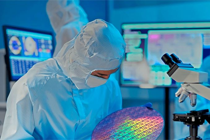

As part of Samsung's Q1 earnings announcement, the company has outlined some of its foundry unit's key plans for the rest of the year. The company has confirmed that it remains on track to meeting its goal of starting mass production of chips on its SF3 (3 nm-class, 2nd Generation) technology in the second half of the year. Meanwhile in June, Samsung Foundry will formally unveil its SF2 (2 nm-class) process technology, which will offer a mix of performance and efficiency enhancements. Finally, the company the company is preparing a variation of its 4 nm-class technology for integration into stacked 3D designs.
Samsung plans to disclose key details about its SF2 fabrication technology at the VLSI Symposium 2024 on June 19. This will be the company's second major process node based upon gate-all-around (GAA) multi-bridge channel field-effect transistors (MBCFET). Improving over its predecessor, SF2 will feature a 'unique epitaxial and integration process,' which will give the process node higher performance and lower leakage than traditional FinFET-based nodes (though Samsung isn't disclosing the specific node they're comparing it to).

Samsung says that SF2 increases performance of narrow transistors by 29% for N-type and 46% for P-type, and wide transistors by 11% and 23% respectively. Moreover, it reduces transistor global variation by 26% compared to FinFET technology, and cuts product leakage by approximately 50%. This process also sets the stage for future advancements in technology through enhanced design technology co-optimization (DTCO) collaboration with its customers.
One thing that Samsung has not mentioned in context of SF2 is backside power delivery, so at least for the moment, there is no indication that Samsung will be adopting this next-gen power routing feature for SF2.
Samsung says that the design infrastructure for SF2 – the PDK, EDA tools, and licensed IP – will be finalized in the second quarter of 2024. Once this happens, Samsung's chip development partners will be able to begin designing products for this production node. Meanwhile, Samsung is already working with Arm to co-optimize Arm's Cortex cores for the SF2 process.
As the first fab to introduce a GAAFET-based node, Samsung has been on the cutting edge of chip construction. At the same time, however, that has also meant that they're the first fab to encounter and solve the inevitable teething issues that come with such a major transistor design change. Consequently, while Samsung's first-generation SF3E process technology has been in production for a little less than two years now, the only publicly-disclosed chips made on the process so far have been relatively small cryptocurrency mining chips – exactly the kind of pipecleaner parts that do well on a new process node.
But with that experience in hand, Samsung is preparing to move on to making bigger and better chips with GAAFETs. As part of their earnings announcements, the company has confirmed that their updated SF3 node, which was introduced last year, remains on schedule to enter production in the second half of 2024.

A more mature product from the get-go, SF3 is being prepared to be used for building larger processors, including datacenter products. Compared to its direct predecessor, SF4, SF3 promises a 22% performance boost at the same power and transistor count, or a 34% lower power at the same frequency and complexity, as well as a 21% logic area reduction. In general, Samsung pins a lot of hopes on this technology, as it's this generation of their 3nm-class technology that is poised to compete against TSMC's N3B and N3E nodes.
Finally, Samsung is also preparing a variant of their final FinFET technology node, SF4, for use in 3D chiplet stacking. As transistor density improvements have continued to slow, 3D chip stacking has emerged as a way to keep boosting overall chip performance, especially with modern, multi-tile processor desig... Semiconductors


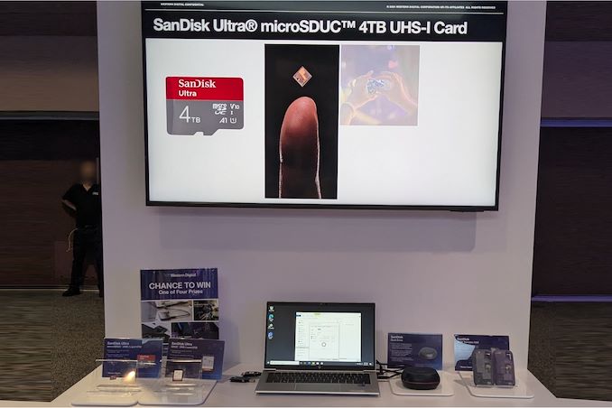
Western Digital's BiCS8 218-layer 3D NAND is being put to good use in a wide range of client and enterprise platforms, including WD's upcoming Gen 5 client SSDs and 128 TB-class datacenter SSD. On the external storage front, the company demonstrated four different products: for card-based media, 4 TB microSDUC and 8 TB SDUC cards with UHS-I speeds, and on the portable SSD front we had two 16 TB drives. One will be a SanDisk Desk Drive with external power, and the other in the SanDisk Extreme Pro housing with a lanyard opening in the case.
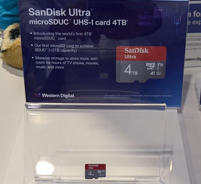
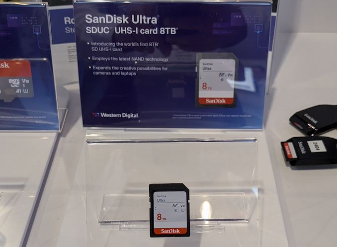
All of these are using BiCS8 QLC NAND, though I did hear booth talk (as I was taking leave) that they were not supposed to divulge the use of QLC in these products. The 4 TB microSDUC and 8 TB SDUC cards are rated for UHS-I speeds. They are being marketed under the SanDisk Ultra branding.
The SanDisk Desk Drive is an external SSD with a 18W power adapter, and it has been in the market for a few months now. Initially launched in capacities up to 8 TB, Western Digital had promised a 16 TB version before the end of the year. It appears that the product is coming to retail quite soon. One aspect to note is that this drive has been using TLC for the SKUs that are currently in the market, so it appears unlikely that the 16 TB version would be QLC. The units (at least up to the 8 TB capacity point) come with two SN850XE drives. Given the recent introduction of the 8 TB SN850X, an 'E' version with tweaked firmware is likely to be present in the 16 TB Desk Drive.
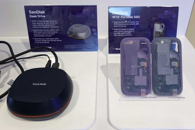
The 16 TB portable SSD in the SanDisk Extreme housing was a technology demonstration. It is definitely the highest capacity bus-powered portable SSD demonstrated by any vendor at any trade show thus far. Given the 16 TB Desk Drive's imminent market introduction, it is just a matter of time before the technology demonstration of the bus-powered version becomes a retail reality.
Storage
The CXL consortium has had a regular presence at FMS (which rechristened itself from 'Flash Memory Summit' to the 'Future of Memory and Storage' this year). Back at FMS 2022, the company had announced v3.0 of the CXL specifications. This was followed by CXL 3.1's introduction at Supercomputing 2023. Having started off as a host to device interconnect standard, it had slowly subsumed other competing standards such as OpenCAPI and Gen-Z. As a result, the specifications started to encompass a wide variety of use-cases by building a protocol on top of the the ubiquitous PCIe expansion bus. The CXL consortium comprises of heavyweights such as AMD and Intel, as well as a large number of startup companies attempting to play in different segments on the device side. At FMS 2024, CXL had a prime position in the booth demos of many vendors.
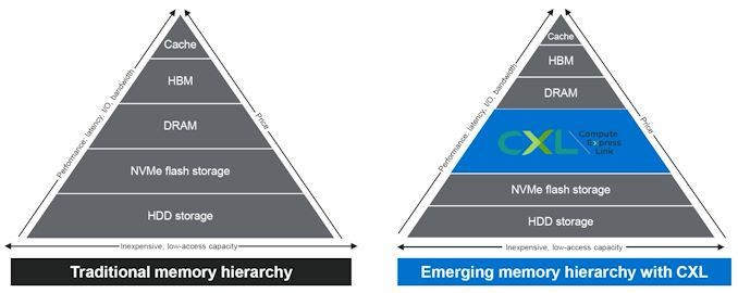
The migration of server platforms from DDR4 to DDR5, along with the rise of workloads demanding large RAM capacity (but not particularly sensitive to either memory bandwidth or latency), has opened up memory expansion modules as one of the first set of widely available CXL devices. Over the last couple of years, we have had product announcements from Samsung and Micron in this area.
At FMS 2024, SK hynix was showing off their DDR5-based CMM-DDR5 CXL memory module with a 128 GB capacity. The company was also detailing their associated Heterogeneous Memory Software Development Kit (HMSDK) - a set of libraries and tools at both the kernel and user levels aimed at increasing the ease of use of CXL memory. This is achieved in part by considering the memory pyramid / hierarchy and relocating the data between the server's main memory (DRAM) and the CXL device based on usage frequency.
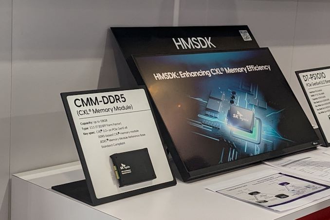
The CMM-DDR5 CXL memory module comes in the SDFF form-factor (E3.S 2T) with a PCIe 3.0 x8 host interface. The internal memory is based on 1α technology DRAM, and the device promises DDR5-class bandwidth and latency within a single NUMA hop. As these memory modules are meant to be used in datacenters and enterprises, the firmware includes features for RAS (reliability, availability, and serviceability) along with secure boot and other management features.
SK hynix was also demonstrating Niagara 2.0 - a hardware solution (currently based on FPGAs) to enable memory pooling and sharing - i.e, connecting multiple CXL memories to allow different hosts (CPUs and GPUs) to optimally share their capacity. The previous version only allowed capacity sharing, but the latest version enables sharing of data also. SK hynix had presented these solutions at the CXL DevCon 2024 earlier this year, but some progress seems to have been made in finalizing the specifications of the CMM-DDR5 at FMS 2024.
Micron had unveiled the CZ120 CXL Memory Expansion Module last year based on the Microchip SMC 2000 series CXL memory controller. At FMS 2024, Micron and Microchip had a demonstration of the module on a Granite Rapids server.
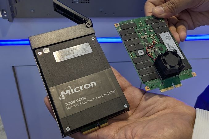
Additional insights into the SMC 2000 controller were also provided.
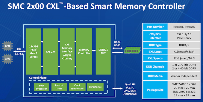
The CXL memory controller also incorporates DRAM die failure handling, and Microchip also provides diagnostics and debug tools to analyze failed modules. The memory controller also supports ECC, which forms part of the enterprise... Storage
Western Digital's BiCS8 218-layer 3D NAND is being put to good use in a wide range of client and enterprise platforms, including WD's upcoming Gen 5 client SSDs and 128 TB-class datacenter SSD. On the external storage front, the company demonstrated four different products: for card-based media, 4 TB microSDUC and 8 TB SDUC cards with UHS-I speeds, and on the portable SSD front we had two 16 TB drives. One will be a SanDisk Desk Drive with external power, and the other in the SanDisk Extreme Pro housing with a lanyard opening in the case.
All of these are using BiCS8 QLC NAND, though I did hear booth talk (as I was taking leave) that they were not supposed to divulge the use of QLC in these products. The 4 TB microSDUC and 8 TB SDUC cards are rated for UHS-I speeds. They are being marketed under the SanDisk Ultra branding.
The SanDisk Desk Drive is an external SSD with a 18W power adapter, and it has been in the market for a few months now. Initially launched in capacities up to 8 TB, Western Digital had promised a 16 TB version before the end of the year. It appears that the product is coming to retail quite soon. One aspect to note is that this drive has been using TLC for the SKUs that are currently in the market, so it appears unlikely that the 16 TB version would be QLC. The units (at least up to the 8 TB capacity point) come with two SN850XE drives. Given the recent introduction of the 8 TB SN850X, an 'E' version with tweaked firmware is likely to be present in the 16 TB Desk Drive.
The 16 TB portable SSD in the SanDisk Extreme housing was a technology demonstration. It is definitely the highest capacity bus-powered portable SSD demonstrated by any vendor at any trade show thus far. Given the 16 TB Desk Drive's imminent market introduction, it is just a matter of time before the technology demonstration of the bus-powered version becomes a retail reality.
Storage
The CXL consortium has had a regular presence at FMS (which rechristened itself from 'Flash Memory Summit' to the 'Future of Memory and Storage' this year). Back at FMS 2022, the company had announced v3.0 of the CXL specifications. This was followed by CXL 3.1's introduction at Supercomputing 2023. Having started off as a host to device interconnect standard, it had slowly subsumed other competing standards such as OpenCAPI and Gen-Z. As a result, the specifications started to encompass a wide variety of use-cases by building a protocol on top of the the ubiquitous PCIe expansion bus. The CXL consortium comprises of heavyweights such as AMD and Intel, as well as a large number of startup companies attempting to play in different segments on the device side. At FMS 2024, CXL had a prime position in the booth demos of many vendors.
The migration of server platforms from DDR4 to DDR5, along with the rise of workloads demanding large RAM capacity (but not particularly sensitive to either memory bandwidth or latency), has opened up memory expansion modules as one of the first set of widely available CXL devices. Over the last couple of years, we have had product announcements from Samsung and Micron in this area.
At FMS 2024, SK hynix was showing off their DDR5-based CMM-DDR5 CXL memory module with a 128 GB capacity. The company was also detailing their associated Heterogeneous Memory Software Development Kit (HMSDK) - a set of libraries and tools at both the kernel and user levels aimed at increasing the ease of use of CXL memory. This is achieved in part by considering the memory pyramid / hierarchy and relocating the data between the server's main memory (DRAM) and the CXL device based on usage frequency.
The CMM-DDR5 CXL memory module comes in the SDFF form-factor (E3.S 2T) with a PCIe 3.0 x8 host interface. The internal memory is based on 1α technology DRAM, and the device promises DDR5-class bandwidth and latency within a single NUMA hop. As these memory modules are meant to be used in datacenters and enterprises, the firmware includes features for RAS (reliability, availability, and serviceability) along with secure boot and other management features.
SK hynix was also demonstrating Niagara 2.0 - a hardware solution (currently based on FPGAs) to enable memory pooling and sharing - i.e, connecting multiple CXL memories to allow different hosts (CPUs and GPUs) to optimally share their capacity. The previous version only allowed capacity sharing, but the latest version enables sharing of data also. SK hynix had presented these solutions at the CXL DevCon 2024 earlier this year, but some progress seems to have been made in finalizing the specifications of the CMM-DDR5 at FMS 2024.
Micron had unveiled the CZ120 CXL Memory Expansion Module last year based on the Microchip SMC 2000 series CXL memory controller. At FMS 2024, Micron and Microchip had a demonstration of the module on a Granite Rapids server.
Additional insights into the SMC 2000 controller were also provided.
The CXL memory controller also incorporates DRAM die failure handling, and Microchip also provides diagnostics and debug tools to analyze failed modules. The memory controller also supports ECC, which forms part of the enterprise... Storage

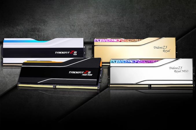
G.Skill on Tuesday introduced its ultra-low-latency DDR5-6400 memory modules that feature a CAS latency of 30 clocks, which appears to be the industry's most aggressive timings yet for DDR5-6400 sticks. The modules will be available for both AMD and Intel CPU-based systems.
With every new generation of DDR memory comes an increase in data transfer rates and an extension of relative latencies. While for the vast majority of applications, the increased bandwidth offsets the performance impact of higher timings, there are applications that favor low latencies. However, shrinking latencies is sometimes harder than increasing data transfer rates, which is why low-latency modules are rare.
Nonetheless, G.Skill has apparently managed to cherry-pick enough DDR5 memory chips and build appropriate printed circuit boards to produce DDR5-6400 modules with CL30 timings, which are substantially lower than the CL46 timings recommended by JEDEC for this speed bin. This means that while JEDEC-standard modules have an absolute latency of 14.375 ns, G.Skill's modules can boast a latency of just 9.375 ns – an approximately 35% decrease.
G.Skill's DDR5-6400 CL30 39-39-102 modules have a capacity of 16 GB and will be available in 32 GB dual-channel kits, though the company does not disclose voltages, which are likely considerably higher than those standardized by JEDEC.
The company plans to make its DDR5-6400 modules available both for AMD systems with EXPO profiles (Trident Z5 Neo RGB and Trident Z5 Royal Neo) and for Intel-powered PCs with XMP 3.0 profiles (Trident Z5 RGB and Trident Z5 Royal). For AMD AM5 systems that have a practical limitation of 6000 MT/s – 6400 MT/s for DDR5 memory (as this is roughly as fast as AMD's Infinity Fabric can operate at with a 1:1 ratio), the new modules will be particularly beneficial for AMD's Ryzen 7000 and Ryzen 9000-series processors.
G.Skill notes that since its modules are non-standard, they will not work with all systems but will operate on high-end motherboards with properly cooled CPUs.
The new ultra-low-latency memory kits will be available worldwide from G.Skill's partners starting in late August 2024. The company did not disclose the pricing of these modules, but since we are talking about premium products that boast unique specifications, they are likely to be priced accordingly.
Memory
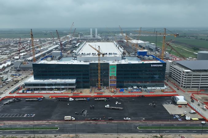
Samsung Electronics this week was awarded up to $6.4 billion from the U.S. government under the CHIPS and Science Act to build its new fab complex in Taylor, Texas. This is the third major award under the act in the last month, with all three leading-edge fabs – Intel, TSMC, and now Samsung – receiving multi-billion dollar funding packages under the domestic chip production program. Overall, the final price tag on Samsung's new fab complex is expected to reach $40 billion by the time it's completed later this decade.
Samsung's CHIPS Act funding was announced during a celebratory event attended by U.S. Secretary of Commerce Gina Raimondo and Samsung Semiconductor chief executive Kye Hyun Kyung. During the event, Kyung outlined the strategic goals of the expansion, emphasizing that the additional funding will not only increase production capacity but also strengthen the entire local semiconductor ecosystem. Samsung plans to equip its fab near Taylor, Texas, with the latest wafer fab tools to produce advanced chips. The Financial Times reports that Samsung aims to produce semiconductors on its 2nm-class process technology starting 2026, though for now this is unofficial information.
"I am pleased to announce a preliminary agreement between Samsung and the Department of Commerce to bring Samsung's advanced semiconductor manufacturing and research and development to Texas," said Joe Biden, the U.S. president, in a statement. "This announcement will unleash over $40 billion in investment from Samsung, and cement central Texas's role as a state-of-the-art semiconductor ecosystem, creating at least 21,500 jobs and leveraging up to $40 million in CHIPS funding to train and develop the local workforce. These facilities will support the production of some of the most powerful chips in the world, which are essential to advanced technologies like artificial intelligence and will bolster U.S. national security."
Samsung has been a significant contributor to the Texas economy for decades, starting chip manufacturing in the U.S. in 1996. With previous investments totaling $18 billion in its Austin operations, Samsung's expansion into Taylor with an additional investment of at least $17 billion underscores its role as one of the largest foreign direct investors in U.S. history. The total expected investment in the new fab surpasses $40 billion, making it one of the largest for a greenfield project in the nation and transforming Taylor into a major hub for semiconductor manufacturing.
The CEO highlighted the substantial economic impact of Samsung's operations, noting a nearly double increase in regional economic output from $13.6 billion to $26.8 billion between 2022 and 2023. The ongoing expansion is projected to further stimulate economic growth, create thousands of jobs, and enhance the community's overall development.
“We are not just expanding production facilities; we’re strengthening the local semiconductor ecosystem and positioning the U.S. as a global semiconductor manufacturing destination.” said Kyung. “To meet the expected surge in demand from U.S. customers, for future products like AI chips, our fabs will be equipped for cutting-edge process technologies and help bring security to the U.S. semiconductor supply chain.”
Samsung is also committed to environmental sustainability and workforce development. The company plans to operate using 100% clean energy and incorporate advanced water management technologies. Additionally, it is investing in education and training programs to develop a new generation of semiconductor professionals. These initiatives include partnerships with educational institutions and programs tailored for military veterans.
In his remarks, Kyung expressed gratitude to President Biden, Secretary Raimondo, and other governmental and community supporters for their ongoing support. This collaborative effort between Samsung and various levels of government, as well as the local community, is pivotal in advancing America's... Semiconductors

Lorem Ipsum is simply dummy text of the printing and typesetting industry. Lorem Ipsum has been the industry's.
Western Digital's BiCS8 218-layer 3D NAND is being put to good use in a wide range of client and enterprise platforms, including WD's upcoming Gen 5 client SSDs and 128 TB-class datacenter SSD. On the external storage front, the company demonstrated four different products: for card-based media, 4 TB microSDUC and 8 TB SDUC cards with UHS-I speeds, and on the portable SSD front we had two 16 TB drives. One will be a SanDisk Desk Drive with external power, and the other in the SanDisk Extreme Pro housing with a lanyard opening in the case.
All of these are using BiCS8 QLC NAND, though I did hear booth talk (as I was taking leave) that they were not supposed to divulge the use of QLC in these products. The 4 TB microSDUC and 8 TB SDUC cards are rated for UHS-I speeds. They are being marketed under the SanDisk Ultra branding.
The SanDisk Desk Drive is an external SSD with a 18W power adapter, and it has been in the market for a few months now. Initially launched in capacities up to 8 TB, Western Digital had promised a 16 TB version before the end of the year. It appears that the product is coming to retail quite soon. One aspect to note is that this drive has been using TLC for the SKUs that are currently in the market, so it appears unlikely that the 16 TB version would be QLC. The units (at least up to the 8 TB capacity point) come with two SN850XE drives. Given the recent introduction of the 8 TB SN850X, an 'E' version with tweaked firmware is likely to be present in the 16 TB Desk Drive.
The 16 TB portable SSD in the SanDisk Extreme housing was a technology demonstration. It is definitely the highest capacity bus-powered portable SSD demonstrated by any vendor at any trade show thus far. Given the 16 TB Desk Drive's imminent market introduction, it is just a matter of time before the technology demonstration of the bus-powered version becomes a retail reality.
Storage





 technology in the second half of the year. Meanwhile in June, Samsung Foundry will formally unveil its SF2 (2 nm-class) process technology, which will offer a mix of performance and efficiency enhancements. Finally, the company the company is preparing a variation of its 4 nm-class technology for integration into stacked 3D designs.</p>
<h3>SF2 To Be Unveiled In June</h3>
<p>Samsung plans to disclose key details about its SF2 fabrication technology at the VLSI Symposium 2024 on June 19. This will be the company's second major process node based upon gate-all-around (GAA) multi-bridge channel field-effect transistors (MBCFET). Improving over its predecessor, SF2 will feature a 'unique epitaxial and integration process,' which will give the process node higher performance and lower leakage than traditional FinFET-based nodes (though Samsung isn't disclosing the specific node they're comparing it to).</p>
<p style="text-align: center;"><a href="https://www.anandtech.com/show/21377/samsung-foundry-update-2nm-unveil-in-june-2nd-gen-3nm-hits-production-this-year"><img alt="" src="https://images.anandtech.com/doci/21377/samsung-foundry-roadmap.png" style="width: 100%;" /></a></p>
<p>Samsung says that SF2 increases performance of narrow transistors by 29% for N-type and 46% for P-type, and wide transistors by 11% and 23% respectively. Moreover, it reduces transistor global variation by 26% compared to FinFET technology, and cuts product leakage by approximately 50%. This process also sets the stage for future advancements in technology through enhanced design technology co-optimization (DTCO) collaboration with its customers.</p>
<p>One thing that Samsung has not mentioned in context of SF2 is backside power delivery, so at least for the moment, there is no indication that Samsung will be adopting this next-gen power routing feature for SF2.</p>
<p>Samsung says that the design infrastructure for SF2 – the PDK, EDA tools, and licensed IP – will be finalized in the second quarter of 2024. Once this happens, Samsung's chip development partners will be able to begin designing products for this production node. Meanwhile, Samsung is already working with Arm to co-optimize Arm's Cortex cores for the SF2 process.</p>
<h3>SF3: On Track for 2H 2024</h3>
<p>As the first fab to introduce a GAAFET-based node, Samsung has been on the cutting edge of chip construction. At the same time, however, that has also meant that they're the first fab to encounter and solve the inevitable teething issues that come with such a major transistor design change. Consequently, while Samsung's first-generation SF3E process technology has been in production for a little less than two years now, the only publicly-disclosed chips made on the process so far have been relatively small cryptocurrency mining chips – exactly the kind of pipecleaner parts that do well on a new process node.</p>
<p>But with that experience in hand, Samsung is preparing to move on to making bigger and better chips with GAAFETs. As part of their earnings announcements, the company has confirmed that their updated SF3 node, which was introduced last year, remains on schedule to enter production in the second half of 2024.</p>
<p align="center"><a href="https://www.anandtech.com/show/21377/samsung-foundry-update-2nm-unveil-in-june-2nd-gen-3nm-hits-production-this-year"><img alt="" src="https://images.anandtech.com/doci/21377/Samsung_Q1_Foundry.png" style="width: 100%;" /></a></p>
<p>A more mature product from the get-go, SF3 is being prepared to be used for building larger processors, including datacenter products. Compared to its direct predecessor, SF4, SF3 promises a 22% performance boost at the same power and transistor count, or a 34% lower power at the same frequency and complexity, as well as a 21% logic area reduction. In general, Samsung pins a lot of hopes on this technology, as it's this generation of their 3nm-class technology that is poised to compete against TSMC's N3B and N3E nodes.</p>
<h3>SF4: Ready for 3D Stacking</h3>
<p>Finally, Samsung is also preparing a variant of their final FinFET technology node, SF4, for use in 3D chiplet stacking. As transistor density improvements have continued to slow, 3D chip stacking has emerged as a way to keep boosting overall chip performance, especially with modern, multi-tile processor desig... Semiconductors)
 technology in the second half of the year. Meanwhile in June, Samsung Foundry will formally unveil its SF2 (2 nm-class) process technology, which will offer a mix of performance and efficiency enhancements. Finally, the company the company is preparing a variation of its 4 nm-class technology for integration into stacked 3D designs.</p>
<h3>SF2 To Be Unveiled In June</h3>
<p>Samsung plans to disclose key details about its SF2 fabrication technology at the VLSI Symposium 2024 on June 19. This will be the company's second major process node based upon gate-all-around (GAA) multi-bridge channel field-effect transistors (MBCFET). Improving over its predecessor, SF2 will feature a 'unique epitaxial and integration process,' which will give the process node higher performance and lower leakage than traditional FinFET-based nodes (though Samsung isn't disclosing the specific node they're comparing it to).</p>
<p style="text-align: center;"><a href="https://www.anandtech.com/show/21377/samsung-foundry-update-2nm-unveil-in-june-2nd-gen-3nm-hits-production-this-year"><img alt="" src="https://images.anandtech.com/doci/21377/samsung-foundry-roadmap.png" style="width: 100%;" /></a></p>
<p>Samsung says that SF2 increases performance of narrow transistors by 29% for N-type and 46% for P-type, and wide transistors by 11% and 23% respectively. Moreover, it reduces transistor global variation by 26% compared to FinFET technology, and cuts product leakage by approximately 50%. This process also sets the stage for future advancements in technology through enhanced design technology co-optimization (DTCO) collaboration with its customers.</p>
<p>One thing that Samsung has not mentioned in context of SF2 is backside power delivery, so at least for the moment, there is no indication that Samsung will be adopting this next-gen power routing feature for SF2.</p>
<p>Samsung says that the design infrastructure for SF2 – the PDK, EDA tools, and licensed IP – will be finalized in the second quarter of 2024. Once this happens, Samsung's chip development partners will be able to begin designing products for this production node. Meanwhile, Samsung is already working with Arm to co-optimize Arm's Cortex cores for the SF2 process.</p>
<h3>SF3: On Track for 2H 2024</h3>
<p>As the first fab to introduce a GAAFET-based node, Samsung has been on the cutting edge of chip construction. At the same time, however, that has also meant that they're the first fab to encounter and solve the inevitable teething issues that come with such a major transistor design change. Consequently, while Samsung's first-generation SF3E process technology has been in production for a little less than two years now, the only publicly-disclosed chips made on the process so far have been relatively small cryptocurrency mining chips – exactly the kind of pipecleaner parts that do well on a new process node.</p>
<p>But with that experience in hand, Samsung is preparing to move on to making bigger and better chips with GAAFETs. As part of their earnings announcements, the company has confirmed that their updated SF3 node, which was introduced last year, remains on schedule to enter production in the second half of 2024.</p>
<p align="center"><a href="https://www.anandtech.com/show/21377/samsung-foundry-update-2nm-unveil-in-june-2nd-gen-3nm-hits-production-this-year"><img alt="" src="https://images.anandtech.com/doci/21377/Samsung_Q1_Foundry.png" style="width: 100%;" /></a></p>
<p>A more mature product from the get-go, SF3 is being prepared to be used for building larger processors, including datacenter products. Compared to its direct predecessor, SF4, SF3 promises a 22% performance boost at the same power and transistor count, or a 34% lower power at the same frequency and complexity, as well as a 21% logic area reduction. In general, Samsung pins a lot of hopes on this technology, as it's this generation of their 3nm-class technology that is poised to compete against TSMC's N3B and N3E nodes.</p>
<h3>SF4: Ready for 3D Stacking</h3>
<p>Finally, Samsung is also preparing a variant of their final FinFET technology node, SF4, for use in 3D chiplet stacking. As transistor density improvements have continued to slow, 3D chip stacking has emerged as a way to keep boosting overall chip performance, especially with modern, multi-tile processor desig... Semiconductors)
 technology in the second half of the year. Meanwhile in June, Samsung Foundry will formally unveil its SF2 (2 nm-class) process technology, which will offer a mix of performance and efficiency enhancements. Finally, the company the company is preparing a variation of its 4 nm-class technology for integration into stacked 3D designs.</p>
<h3>SF2 To Be Unveiled In June</h3>
<p>Samsung plans to disclose key details about its SF2 fabrication technology at the VLSI Symposium 2024 on June 19. This will be the company's second major process node based upon gate-all-around (GAA) multi-bridge channel field-effect transistors (MBCFET). Improving over its predecessor, SF2 will feature a 'unique epitaxial and integration process,' which will give the process node higher performance and lower leakage than traditional FinFET-based nodes (though Samsung isn't disclosing the specific node they're comparing it to).</p>
<p style="text-align: center;"><a href="https://www.anandtech.com/show/21377/samsung-foundry-update-2nm-unveil-in-june-2nd-gen-3nm-hits-production-this-year"><img alt="" src="https://images.anandtech.com/doci/21377/samsung-foundry-roadmap.png" style="width: 100%;" /></a></p>
<p>Samsung says that SF2 increases performance of narrow transistors by 29% for N-type and 46% for P-type, and wide transistors by 11% and 23% respectively. Moreover, it reduces transistor global variation by 26% compared to FinFET technology, and cuts product leakage by approximately 50%. This process also sets the stage for future advancements in technology through enhanced design technology co-optimization (DTCO) collaboration with its customers.</p>
<p>One thing that Samsung has not mentioned in context of SF2 is backside power delivery, so at least for the moment, there is no indication that Samsung will be adopting this next-gen power routing feature for SF2.</p>
<p>Samsung says that the design infrastructure for SF2 – the PDK, EDA tools, and licensed IP – will be finalized in the second quarter of 2024. Once this happens, Samsung's chip development partners will be able to begin designing products for this production node. Meanwhile, Samsung is already working with Arm to co-optimize Arm's Cortex cores for the SF2 process.</p>
<h3>SF3: On Track for 2H 2024</h3>
<p>As the first fab to introduce a GAAFET-based node, Samsung has been on the cutting edge of chip construction. At the same time, however, that has also meant that they're the first fab to encounter and solve the inevitable teething issues that come with such a major transistor design change. Consequently, while Samsung's first-generation SF3E process technology has been in production for a little less than two years now, the only publicly-disclosed chips made on the process so far have been relatively small cryptocurrency mining chips – exactly the kind of pipecleaner parts that do well on a new process node.</p>
<p>But with that experience in hand, Samsung is preparing to move on to making bigger and better chips with GAAFETs. As part of their earnings announcements, the company has confirmed that their updated SF3 node, which was introduced last year, remains on schedule to enter production in the second half of 2024.</p>
<p align="center"><a href="https://www.anandtech.com/show/21377/samsung-foundry-update-2nm-unveil-in-june-2nd-gen-3nm-hits-production-this-year"><img alt="" src="https://images.anandtech.com/doci/21377/Samsung_Q1_Foundry.png" style="width: 100%;" /></a></p>
<p>A more mature product from the get-go, SF3 is being prepared to be used for building larger processors, including datacenter products. Compared to its direct predecessor, SF4, SF3 promises a 22% performance boost at the same power and transistor count, or a 34% lower power at the same frequency and complexity, as well as a 21% logic area reduction. In general, Samsung pins a lot of hopes on this technology, as it's this generation of their 3nm-class technology that is poised to compete against TSMC's N3B and N3E nodes.</p>
<h3>SF4: Ready for 3D Stacking</h3>
<p>Finally, Samsung is also preparing a variant of their final FinFET technology node, SF4, for use in 3D chiplet stacking. As transistor density improvements have continued to slow, 3D chip stacking has emerged as a way to keep boosting overall chip performance, especially with modern, multi-tile processor desig... Semiconductors | https://compbuddey.blogspot.com/2024/05/samsung-foundry-update-2nm-unveil-in_16.html)
 technology in the second half of the year. Meanwhile in June, Samsung Foundry will formally unveil its SF2 (2 nm-class) process technology, which will offer a mix of performance and efficiency enhancements. Finally, the company the company is preparing a variation of its 4 nm-class technology for integration into stacked 3D designs.</p>
<h3>SF2 To Be Unveiled In June</h3>
<p>Samsung plans to disclose key details about its SF2 fabrication technology at the VLSI Symposium 2024 on June 19. This will be the company's second major process node based upon gate-all-around (GAA) multi-bridge channel field-effect transistors (MBCFET). Improving over its predecessor, SF2 will feature a 'unique epitaxial and integration process,' which will give the process node higher performance and lower leakage than traditional FinFET-based nodes (though Samsung isn't disclosing the specific node they're comparing it to).</p>
<p style="text-align: center;"><a href="https://www.anandtech.com/show/21377/samsung-foundry-update-2nm-unveil-in-june-2nd-gen-3nm-hits-production-this-year"><img alt="" src="https://images.anandtech.com/doci/21377/samsung-foundry-roadmap.png" style="width: 100%;" /></a></p>
<p>Samsung says that SF2 increases performance of narrow transistors by 29% for N-type and 46% for P-type, and wide transistors by 11% and 23% respectively. Moreover, it reduces transistor global variation by 26% compared to FinFET technology, and cuts product leakage by approximately 50%. This process also sets the stage for future advancements in technology through enhanced design technology co-optimization (DTCO) collaboration with its customers.</p>
<p>One thing that Samsung has not mentioned in context of SF2 is backside power delivery, so at least for the moment, there is no indication that Samsung will be adopting this next-gen power routing feature for SF2.</p>
<p>Samsung says that the design infrastructure for SF2 – the PDK, EDA tools, and licensed IP – will be finalized in the second quarter of 2024. Once this happens, Samsung's chip development partners will be able to begin designing products for this production node. Meanwhile, Samsung is already working with Arm to co-optimize Arm's Cortex cores for the SF2 process.</p>
<h3>SF3: On Track for 2H 2024</h3>
<p>As the first fab to introduce a GAAFET-based node, Samsung has been on the cutting edge of chip construction. At the same time, however, that has also meant that they're the first fab to encounter and solve the inevitable teething issues that come with such a major transistor design change. Consequently, while Samsung's first-generation SF3E process technology has been in production for a little less than two years now, the only publicly-disclosed chips made on the process so far have been relatively small cryptocurrency mining chips – exactly the kind of pipecleaner parts that do well on a new process node.</p>
<p>But with that experience in hand, Samsung is preparing to move on to making bigger and better chips with GAAFETs. As part of their earnings announcements, the company has confirmed that their updated SF3 node, which was introduced last year, remains on schedule to enter production in the second half of 2024.</p>
<p align="center"><a href="https://www.anandtech.com/show/21377/samsung-foundry-update-2nm-unveil-in-june-2nd-gen-3nm-hits-production-this-year"><img alt="" src="https://images.anandtech.com/doci/21377/Samsung_Q1_Foundry.png" style="width: 100%;" /></a></p>
<p>A more mature product from the get-go, SF3 is being prepared to be used for building larger processors, including datacenter products. Compared to its direct predecessor, SF4, SF3 promises a 22% performance boost at the same power and transistor count, or a 34% lower power at the same frequency and complexity, as well as a 21% logic area reduction. In general, Samsung pins a lot of hopes on this technology, as it's this generation of their 3nm-class technology that is poised to compete against TSMC's N3B and N3E nodes.</p>
<h3>SF4: Ready for 3D Stacking</h3>
<p>Finally, Samsung is also preparing a variant of their final FinFET technology node, SF4, for use in 3D chiplet stacking. As transistor density improvements have continued to slow, 3D chip stacking has emerged as a way to keep boosting overall chip performance, especially with modern, multi-tile processor desig... Semiconductors&body=https://compbuddey.blogspot.com/2024/05/samsung-foundry-update-2nm-unveil-in_16.html)


0 Comments