
UPDATE 5/17, 6 PM: Western Digital has confirmed that the new 2.5-inch T GB HDDs uses 6 SMR platters
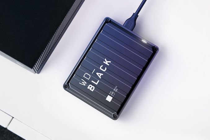
The vast majority of laptops nowadays use solid-state drives, which is why the development of new, higher-capacity 2.5-inch hard drives has all but come to a halt. Or rather, it almost has. It seems that the 2.5-inch form factor has a bit more life left in it after all, as today Western Digital has released a slate of new external storage products based on a new, high-capacity 6 TB 2.5-inch hard drive.
WD's new 6 TB spinner is being used to offer upgraded versions of the company's My Passport, Black P10, and and G-DRIVE ArmorATD portable storage products. Notably, however, WD isn't selling the bare 2.5-inch drive on a standalone basis – at least not yet – so for the time being it's entirely reserved for use in external storage.
Consequently, WD isn't publishing much about the 6 TB hard drive itself. The maximum read speed for these products is listed at 130 MB/sec – the same as WD's existing externals – and write performance goes unmentioned.
Notably, all of these 6 TB devices are thicker than their existing 5 TB counterparts, which strongly suggests that WD has increased their storage capacity not by improving their areal density, but by adding another platter to their existing drive platform (which WD has since confirmed). This, in turn, would help to explain why these new drives are being used in external storage products, as WD's 5 TB 2.5-inch drives are already 15mm thick and using 5 platters. 15mm is the highest standard thickness for a 2.5-inch form-factor, and already incompatible with a decent number of portable devices. External drives, in turn, are the only place these even thicker 2.5-inch drives would fit.
WD's specifications also gloss over whether these drives are based on shingled magnetic recording (SMR) technology. The company was already using SMR for their 5 TB drives in order to hit the necessary storage density there, and WD has since confirmed that this is exactly the case. Which is likely why the company isn't publishing write performance specifications for the drives, as we've seen device-managed SMR drives bottom out as low as 10 MB/second in our testing when the drive needs to rewrite data.
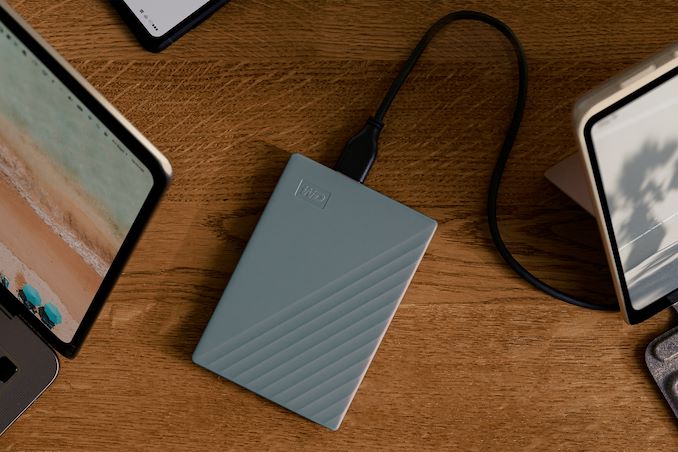
Depending on the specific drive model, all of the external storage drives use either a USB-C connector, or the very quaint USB Micro-B 3.0 connector. Though regardless of the physical connector used, all of the drives feature a USB 3.2 Gen 1 (5Gbps) electrical interface, which is more than ample given the drives' physically-limited transfer speeds.
Wrapping things up, according to WD the new drives are available at retail immediately. The WD My Passport Ultra and WD My Passport Ultra for Mac with USB-C both retail for $199.99; the WD My Passport and WD My Passport for Mac are $179.99; the WD My Passport Works With USB-C is $184.99; the gaming-focused WD_Black P10 Game Drive sells for $184.99, and the SanDisk Professional G-Drive ArmorATD is $229.99. All of Western Digital's external storage drives are backed with a three-year limited warranty.
Storage

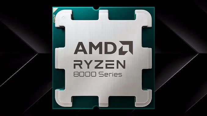
AMD has recently expanded its Ryzen 8000 series by introducing the Ryzen 7 8700F and Ryzen 5 8400F processors. Initially launched in China, these chips were added to AMD's global website, signaling they are available worldwide, apparently from April 1st. Built from the recent Zen 4-based Phoenix APUs using the TSMC 4nm node as their Zen 4 mobile chips, these new CPUs lack integrated graphics. However, the Ryzen 7 8700F does include the integrated Ryzen AI NPU for added capabilities in a world currently dominated by AI and moving it directly into the PC.
The company's decision to announce these chips in China aligns with its strategy to offer Ryzen solutions at every price point in the market. Although AMD didn't initially disclose the full specifications of these F-series models, and we did reach out to the company to ask about them, they refused to discuss them with us. Their listing on the website has now been updated with a complete list of specifications and features, with everything but the price mentioned.
| AMD Ryzen 8000G vs. Ryzen 8000F Series (Desktop) Zen 4 (Phoenix) |
|||||||||
| AnandTech | Cores/Threads | Base Freq |
Turbo Freq |
GPU | GPU Freq |
Ryzen AI (NPU) |
L3 Cache (MB) |
TDP | MSRP |
| Ryzen 7 | |||||||||
| Ryzen 7 8700G | 8/16 | 4200 | 5100 | R780M 12 CUs |
2900 | Y | 16 | 65W | $329 |
| Ryzen 7 8700F | 8/16 | 4100 | 5000 | - | - | Y | 16 | 65W | ? |
| Ryzen 5 | |||||||||
| Ryzen 5 8600G | 6/12 | 4300 | 5000 | R760M 8 CUs |
2800 | Y | 16 | 65W | $229 |
| Ryzen 5 8400F | 6/12 | 4200 | 4700 | - | - | N | 16 | 65W | ? |
The Ryzen 7 8700F features an 8C/16T design, with 16MB of L3 cache and the same 65W TDP as the Ryzen 7 8700G. Although the base clock speed is 4.1 GHz, it boosts to 5.0 GHz; this is 100 MHz less on both base/boost clocks than the 8700G. Meanwhile, the Ryzen 5 8400F is a slightly scaled-down version of the Ryzen 8600G APU, with 6C/12, 16MB of L3 cache, and again has a 100 MHz reduction to base clocks compared to the 8600G. Unlike the Ryzen 5 8400F, the Ryzen 7 8700F keeps AMD's Ryzen AI NPU, adding additional capability for generative AI.
The Ryzen 5 8400F can boost up to 4.7 GHz, 300 MHz slower than the Ryzen 5 8600G. AMD also allows overclocking for these new F-series chips, which means users could potentially boost the performance of these processors to match their G-series equivalents.
Pricing details are still pending, but to remain competitive, AMD will likely need to price these CPUs below the 8700G and 8600G, as well as the Ryzen 7 7700 and Ryzen 5 7600. These CPUs offer, albeit very limited, integrated graphics and have double the L3 cache capacity, along with higher boost clocks than the 8000F series chips, so pricing is something to consider whenever pricing becomes available.
CPUs
AMD has recently expanded its Ryzen 8000 series by introducing the Ryzen 7 8700F and Ryzen 5 8400F processors. Initially launched in China, these chips were added to AMD's global website, signaling they are available worldwide, apparently from April 1st. Built from the recent Zen 4-based Phoenix APUs using the TSMC 4nm node as their Zen 4 mobile chips, these new CPUs lack integrated graphics. However, the Ryzen 7 8700F does include the integrated Ryzen AI NPU for added capabilities in a world currently dominated by AI and moving it directly into the PC.
The company's decision to announce these chips in China aligns with its strategy to offer Ryzen solutions at every price point in the market. Although AMD didn't initially disclose the full specifications of these F-series models, and we did reach out to the company to ask about them, they refused to discuss them with us. Their listing on the website has now been updated with a complete list of specifications and features, with everything but the price mentioned.
| AMD Ryzen 8000G vs. Ryzen 8000F Series (Desktop) Zen 4 (Phoenix) |
|||||||||
| AnandTech | Cores/Threads | Base Freq |
Turbo Freq |
GPU | GPU Freq |
Ryzen AI (NPU) |
L3 Cache (MB) |
TDP | MSRP |
| Ryzen 7 | |||||||||
| Ryzen 7 8700G | 8/16 | 4200 | 5100 | R780M 12 CUs |
2900 | Y | 16 | 65W | $329 |
| Ryzen 7 8700F | 8/16 | 4100 | 5000 | - | - | Y | 16 | 65W | ? |
| Ryzen 5 | |||||||||
| Ryzen 5 8600G | 6/12 | 4300 | 5000 | R760M 8 CUs |
2800 | Y | 16 | 65W | $229 |
| Ryzen 5 8400F | 6/12 | 4200 | 4700 | - | - | N | 16 | 65W | ? |
The Ryzen 7 8700F features an 8C/16T design, with 16MB of L3 cache and the same 65W TDP as the Ryzen 7 8700G. Although the base clock speed is 4.1 GHz, it boosts to 5.0 GHz; this is 100 MHz less on both base/boost clocks than the 8700G. Meanwhile, the Ryzen 5 8400F is a slightly scaled-down version of the Ryzen 8600G APU, with 6C/12, 16MB of L3 cache, and again has a 100 MHz reduction to base clocks compared to the 8600G. Unlike the Ryzen 5 8400F, the Ryzen 7 8700F keeps AMD's Ryzen AI NPU, adding additional capability for generative AI.
The Ryzen 5 8400F can boost up to 4.7 GHz, 300 MHz slower than the Ryzen 5 8600G. AMD also allows overclocking for these new F-series chips, which means users could potentially boost the performance of these processors to match their G-series equivalents.
Pricing details are still pending, but to remain competitive, AMD will likely need to price these CPUs below the 8700G and 8600G, as well as the Ryzen 7 7700 and Ryzen 5 7600. These CPUs offer, albeit very limited, integrated graphics and have double the L3 cache capacity, along with higher boost clocks than the 8000F series chips, so pricing is something to consider whenever pricing becomes available.
CPUs
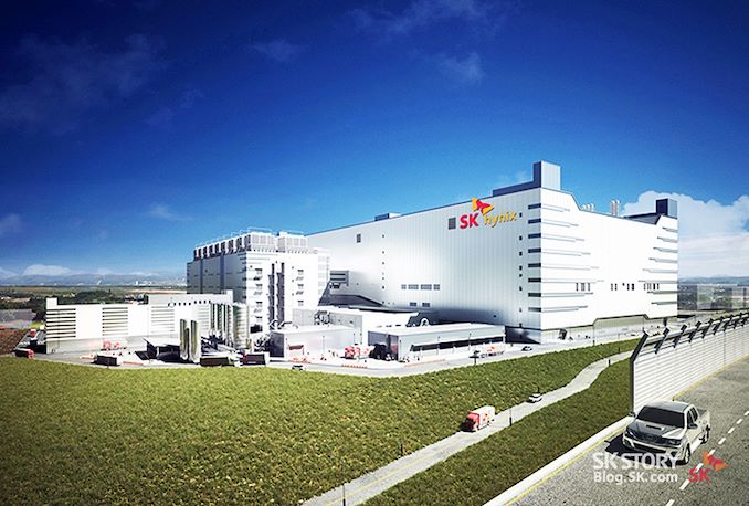
When a major industry slowdown occurs, big companies tend to slowdown their mid-term and long-term capacity related investments. This is exactly what happened to SK hynix's Yongin Semiconductor Cluster, a major project announced in April 2021 and valued at $106 billion. While development of the site has been largely completed, only 35% of the initial shell building has been constructed, according to the Korean Ministry of Trade, Industry, and Energy.
"Approximately 35% of Fab 1 has been completed so far and site renovation is in smooth progress," a statement by the Korean Ministry of Trade, Industry, and Energy reads. "By 2046, over KRW 120 trillion ($90 billion today, $106 billion in 2021) in investment will be poured to complete Fabs 1 through 4, and construction of Fab 1's production line will commence in March next year. Once completed, the infrastructure will rank as the world's largest three-story fab."
The new semiconductor fabrication cluster by SK hynix announced almost exactly three years ago is primarily meant to be used to make DRAM for PCs, mobile devices, and servers using advanced extreme ultraviolet lithography (EUV) process technologies. The cluster, located near Yongin, South Korea, is intended to consist of four large fabs situated on a 4.15 million m2 site. With a planned capacity of approximately 800,000 wafer starts per month (WSPMs), it is set to be one of the world's largest semiconductor production hubs.
With that said, SK hynix's construction progress has been slower than the company first projected. The first fab in the complex was originally meant to come online in 2025, with construction starting in the fourth quarter of 2021. However, SK hynix began to cut its capital expenditures in the second half of 2022, and the Yongin Semiconductor Cluster project fell a victim of that cut. To be sure, the site continues to be developed, just at a slower pace; which is why some 35% of the first fab shell has been built at this point.
If completed as planned in 2021, the first phase of SK hynix Yongin operations would have been a major memory production facility costing $25 billion, equipped with EUV tools, and capable of 200,000-WSPM, according to reports from 2021.
Sources: Korean Ministry of Trade, Industry, and Energy; ComputerBase
Memory
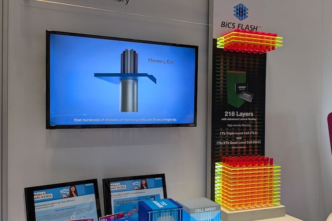
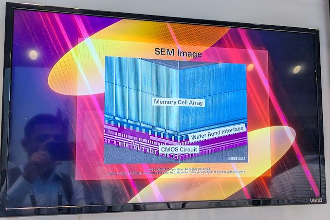
Kioxia's booth at FMS 2024 was a busy one with multiple technology demonstrations keeping visitors occupied. A walk-through of the BiCS 8 manufacturing process was the first to grab my attention. Kioxia and Western Digital announced the sampling of BiCS 8 in March 2023. We had touched briefly upon its CMOS Bonded Array (CBA) scheme in our coverage of Kioxial's 2Tb QLC NAND device and coverage of Western Digital's 128 TB QLC enterprise SSD proof-of-concept demonstration. At Kioxia's booth, we got more insights.
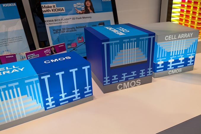
Traditionally, fabrication of flash chips involved placement of the associate logic circuitry (CMOS process) around the periphery of the flash array. The process then moved on to putting the CMOS under the cell array, but the wafer development process was serialized with the CMOS logic getting fabricated first followed by the cell array on top. However, this has some challenges because the cell array requires a high-temperature processing step to ensure higher reliability that can be detrimental to the health of the CMOS logic. Thanks to recent advancements in wafer bonding techniques, the new CBA process allows the CMOS wafer and cell array wafer to be processed independently in parallel and then pieced together, as shown in the models above.
The BiCS 8 3D NAND incorporates 218 layers, compared to 112 layers in BiCS 5 and 162 layers in BiCS 6. The company decided to skip over BiCS 7 (or, rather, it was probably a short-lived generation meant as an internal test vehicle). The generation retains the four-plane charge trap structure of BiCS 6. In its TLC avatar, it is available as a 1 Tbit device. The QLC version is available in two capacities - 1 Tbit and 2 Tbit.
Kioxia also noted that while the number of layers (218) doesn't compare favorably with the latest layer counts from the competition, its lateral scaling / cell shrinkage has enabled it to be competitive in terms of bit density as well as operating speeds (3200 MT/s). For reference, the latest shipping NAND from Micron - the G9 - has 276 layers with a bit density in TLC mode of 21 Gbit/mm2, and operates at up to 3600 MT/s. However, its 232L NAND operates only up to 2400 MT/s and has a bit density of 14.6 Gbit/mm2.
It must be noted that the CBA hybrid bonding process has advantages over the current processes used by other vendors - including Micron's CMOS under array (CuA) and SK hynix's 4D PUC (periphery-under-chip) developed in the late 2010s. It is expected that other NAND vendors will also move eventually to some variant of the hybrid bonding scheme used by Kioxia.
Storage
Lorem Ipsum is simply dummy text of the printing and typesetting industry. Lorem Ipsum has been the industry's.


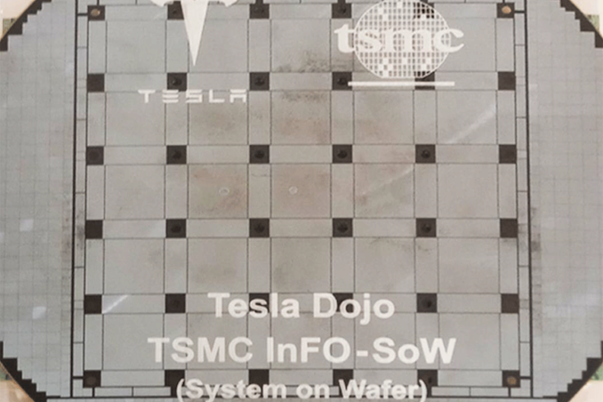
![TSMC's System-on-Wafer Platform Goes 3D: CoW-SoW Stacks Up the Chips <p align="center"><a href="https://www.anandtech.com/show/21372/tsmcs-system-on-wafer-platform-goes-3d-cow-sow"><img src="https://images.anandtech.com/doci/21372/tsmc-sow-tesla-dojo-678_575px.png" alt="" /></a></p><p><p>TSMC has been offering its System-on-Wafer integration technology, InFO-SoW, since 2020. For now, only Cerebras and Tesla have developed wafer scale processor designs using it, as while they have fantastic performance and power efficiency, wafer-scale processors are extremely complex to develop and produce. But TSMC believes that not only will wafer-scale designs ramp up in usage, but that megatrends like AI and HPC will call for even more complex solutions: vertically stacked system-on-wafer designs.</p>
<p style="text-align: center;"><a href="https://www.anandtech.com/show/21372/tsmcs-system-on-wafer-platform-goes-3d-cow-sow"><img alt="" src="https://images.anandtech.com/doci/21372/tsmc-sow-tesla-dojo-575px.png" /></a></p>
<p>Tesla Dojo's wafer-scale processors — the first solutions based based on TSMC's InFO-SoW technology that are in mass production — have a number of benefits over typical system-in-packages (SiPs), including low-latency high-bandwidth core-to-core communications, very high performance and bandwidth density, relatively low power delivery network impendance, high performance efficiency, and redunancy.</p>
<p>But with InFO-SoW and other wafer scale integration methods, processor designers have to rely solely on on-chip memory. This is perfectly adequate for many applications, but it may not be enough for next-generation AI workloads. Furthermore, with InFO-SoW, the whole wafer has to be processed using one fabrication technology, which may not be optimal, or too expensive for certain designs.</p>
<p style="text-align: center;"><a href="https://www.anandtech.com/show/21372/tsmcs-system-on-wafer-platform-goes-3d-cow-sow"><img alt="" src="https://images.anandtech.com/doci/21372/tsmc-sow-cowos-evolution-575px.png" /></a></p>
<p>So, with its next-generation system-on-wafer platform, TSMC plans to bring together two of its packaging technologies: InFO-SoW and System on Integrated Chips (SoIC), which will allow it to stack memory or logic on top of a system-on-wafer using its Chip-on-Wafer (CoW) method. The CoW-SoW technology, which the company announced at its North American Technology Symposium, will be ready for mass production in 2027.</p>
<p>For now, TSMC is mostly talking about wedding wafer scale processors with HBM4 memory. And given that HBM4 stacks will feature a 2048-bit interface, its tighter integration with logic is something that the industry is considering.</p>
<p>"So, in the future, using wafer level integrations [will allow] our customers to integrate even more logic and memory together," said Kevin Zhang, Vice President of Business Development at TSMC. "SoW is no longer a fiction, this is something we already work with our customers [on] to produce some of the products already in place. This we think by leveraging our advanced wafer level integration technology, we can provide our customer a very important the path allow them to continue to grow their capability to bring in more computation, more energy efficient computation, to their AI cluster or [supercomputer]."</p>
<h3><strong>Related Reading</strong></h3>
<ul>
<li><a href="https://www.anandtech.com/show/21369/tsmcs-16nm-technology-announced-for-late-2026-a16-with-super-power-rail-bspdn">TSMC's 1.6nm Technology Announced for Late 2026: A16 with "Super Power Rail" Backside Power</a></li>
<li><a href="https://www.anandtech.com/show/21370/tsmc-2nm-update-n2-in-2025-n2p-loses-bspdn-nanoflex-optimizations">TSMC 2nm Update: N2 In 2025, N2P Loses Backside Power, and NanoFlex Brings Optimal Cells</a></li>
<li><a href="https://www.anandtech.com/show/21371/tsmc-preps-lower-cost-4nm-n4c-process-for-2025">TSMC Preps Cheaper 4nm N4C Process For 2025, Aiming For 8.5% Cost Reduction</a></li>
</ul>
</p> Semiconductors](https://lh3.googleusercontent.com/blogger_img_proxy/AEn0k_v-Rv235wKgdvV6_UGBcGbHO5huuZhq5SRbKVMS_LBxj4T81ovnVLRCiFGu5WvGF8fN64lfK0_uNkeam0LjQkrljAFm0BId696mytPpP39HTVR_H4tXuRgA9KQKZhGGLiwygMK8QEKF0Phsykg=w72-h72-p-k-no-nu)


. This, in turn, would help to explain why these new drives are being used in external storage products, as WD's 5 TB 2.5-inch drives are already 15mm thick and using 5 platters. 15mm is the highest standard thickness for a 2.5-inch form-factor, and already incompatible with a decent number of portable devices. External drives, in turn, are the only place these even thicker 2.5-inch drives would fit.</p>
<p>WD's specifications also gloss over whether these drives are based on shingled magnetic recording (SMR) technology. The company was already using SMR for their 5 TB drives in order to hit the necessary storage density there, and WD has since confirmed that this is exactly the case. Which is likely why the company isn't publishing write performance specifications for the drives, as we've seen device-managed SMR drives bottom out as low as 10 MB/second in our testing when the drive needs to rewrite data.</p>
<p style="text-align: center;"><a href="https://www.anandtech.com/show/21400/not-dead-yet-wd-intros-6tb-25-inch-external-hard-drives"><img alt="" src="https://images.anandtech.com/doci/21400/MyPassportWorksWithUSB-C_SiliconGrey-Universal_Connectivity-678_575px.jpg" /></a></p>
<p>Depending on the specific drive model, all of the external storage drives use either a USB-C connector, or the very quaint USB Micro-B 3.0 connector. Though regardless of the physical connector used, all of the drives feature a USB 3.2 Gen 1 (5Gbps) electrical interface, which is more than ample given the drives' physically-limited transfer speeds.</p>
<p>Wrapping things up, according to WD the new drives are available at retail immediately. The WD My Passport Ultra and WD My Passport Ultra for Mac with USB-C both retail for <a href="https://www.anrdoezrs.net/click-8900248-15168098?sid=anandtech-us-1190245318091501030&url=https://www.westerndigital.com/products/portable-drives/wd-my-passport-ultra-usb-c-hdd?sku=WDBEJA0060BBL-WESN">$199.99</a>; the WD My Passport and WD My Passport for Mac are <a href="https://www.anrdoezrs.net/click-8900248-15168098?sid=anandtech-us-5754388983767137215&url=https://www.westerndigital.com/products/portable-drives/wd-my-passport-usb-3-0-hdd?sku=WDBR9S0060BBK-WESN">$179.99</a>; the WD My Passport Works With USB-C is $184.99; the gaming-focused WD_Black P10 Game Drive sells for <a href="https://www.anrdoezrs.net/click-8900248-15168098?sid=anandtech-us-7306428376444724985&url=https://www.westerndigital.com/products/portable-drives/wd-black-p10-game-drive-usb-3-2-hdd?sku=WDBZ7D0060BBK-WESN">$184.99</a>, and the SanDisk Professional G-Drive ArmorATD is <a href="https://www.anrdoezrs.net/click-8900248-15168098?sid=anandtech-us-9466307572497191337&url=https://www.westerndigital.com/products/portable-drives/sandisk-professional-g-drive-armoratd-usb-3-1-hdd?sku=SDPHE1G-006T-GBAND">$229.99</a>. All of Western Digital's external storage drives are backed with a three-year limited warranty.</p>
</p> Storage)
. This, in turn, would help to explain why these new drives are being used in external storage products, as WD's 5 TB 2.5-inch drives are already 15mm thick and using 5 platters. 15mm is the highest standard thickness for a 2.5-inch form-factor, and already incompatible with a decent number of portable devices. External drives, in turn, are the only place these even thicker 2.5-inch drives would fit.</p>
<p>WD's specifications also gloss over whether these drives are based on shingled magnetic recording (SMR) technology. The company was already using SMR for their 5 TB drives in order to hit the necessary storage density there, and WD has since confirmed that this is exactly the case. Which is likely why the company isn't publishing write performance specifications for the drives, as we've seen device-managed SMR drives bottom out as low as 10 MB/second in our testing when the drive needs to rewrite data.</p>
<p style="text-align: center;"><a href="https://www.anandtech.com/show/21400/not-dead-yet-wd-intros-6tb-25-inch-external-hard-drives"><img alt="" src="https://images.anandtech.com/doci/21400/MyPassportWorksWithUSB-C_SiliconGrey-Universal_Connectivity-678_575px.jpg" /></a></p>
<p>Depending on the specific drive model, all of the external storage drives use either a USB-C connector, or the very quaint USB Micro-B 3.0 connector. Though regardless of the physical connector used, all of the drives feature a USB 3.2 Gen 1 (5Gbps) electrical interface, which is more than ample given the drives' physically-limited transfer speeds.</p>
<p>Wrapping things up, according to WD the new drives are available at retail immediately. The WD My Passport Ultra and WD My Passport Ultra for Mac with USB-C both retail for <a href="https://www.anrdoezrs.net/click-8900248-15168098?sid=anandtech-us-1190245318091501030&url=https://www.westerndigital.com/products/portable-drives/wd-my-passport-ultra-usb-c-hdd?sku=WDBEJA0060BBL-WESN">$199.99</a>; the WD My Passport and WD My Passport for Mac are <a href="https://www.anrdoezrs.net/click-8900248-15168098?sid=anandtech-us-5754388983767137215&url=https://www.westerndigital.com/products/portable-drives/wd-my-passport-usb-3-0-hdd?sku=WDBR9S0060BBK-WESN">$179.99</a>; the WD My Passport Works With USB-C is $184.99; the gaming-focused WD_Black P10 Game Drive sells for <a href="https://www.anrdoezrs.net/click-8900248-15168098?sid=anandtech-us-7306428376444724985&url=https://www.westerndigital.com/products/portable-drives/wd-black-p10-game-drive-usb-3-2-hdd?sku=WDBZ7D0060BBK-WESN">$184.99</a>, and the SanDisk Professional G-Drive ArmorATD is <a href="https://www.anrdoezrs.net/click-8900248-15168098?sid=anandtech-us-9466307572497191337&url=https://www.westerndigital.com/products/portable-drives/sandisk-professional-g-drive-armoratd-usb-3-1-hdd?sku=SDPHE1G-006T-GBAND">$229.99</a>. All of Western Digital's external storage drives are backed with a three-year limited warranty.</p>
</p> Storage)
. This, in turn, would help to explain why these new drives are being used in external storage products, as WD's 5 TB 2.5-inch drives are already 15mm thick and using 5 platters. 15mm is the highest standard thickness for a 2.5-inch form-factor, and already incompatible with a decent number of portable devices. External drives, in turn, are the only place these even thicker 2.5-inch drives would fit.</p>
<p>WD's specifications also gloss over whether these drives are based on shingled magnetic recording (SMR) technology. The company was already using SMR for their 5 TB drives in order to hit the necessary storage density there, and WD has since confirmed that this is exactly the case. Which is likely why the company isn't publishing write performance specifications for the drives, as we've seen device-managed SMR drives bottom out as low as 10 MB/second in our testing when the drive needs to rewrite data.</p>
<p style="text-align: center;"><a href="https://www.anandtech.com/show/21400/not-dead-yet-wd-intros-6tb-25-inch-external-hard-drives"><img alt="" src="https://images.anandtech.com/doci/21400/MyPassportWorksWithUSB-C_SiliconGrey-Universal_Connectivity-678_575px.jpg" /></a></p>
<p>Depending on the specific drive model, all of the external storage drives use either a USB-C connector, or the very quaint USB Micro-B 3.0 connector. Though regardless of the physical connector used, all of the drives feature a USB 3.2 Gen 1 (5Gbps) electrical interface, which is more than ample given the drives' physically-limited transfer speeds.</p>
<p>Wrapping things up, according to WD the new drives are available at retail immediately. The WD My Passport Ultra and WD My Passport Ultra for Mac with USB-C both retail for <a href="https://www.anrdoezrs.net/click-8900248-15168098?sid=anandtech-us-1190245318091501030&url=https://www.westerndigital.com/products/portable-drives/wd-my-passport-ultra-usb-c-hdd?sku=WDBEJA0060BBL-WESN">$199.99</a>; the WD My Passport and WD My Passport for Mac are <a href="https://www.anrdoezrs.net/click-8900248-15168098?sid=anandtech-us-5754388983767137215&url=https://www.westerndigital.com/products/portable-drives/wd-my-passport-usb-3-0-hdd?sku=WDBR9S0060BBK-WESN">$179.99</a>; the WD My Passport Works With USB-C is $184.99; the gaming-focused WD_Black P10 Game Drive sells for <a href="https://www.anrdoezrs.net/click-8900248-15168098?sid=anandtech-us-7306428376444724985&url=https://www.westerndigital.com/products/portable-drives/wd-black-p10-game-drive-usb-3-2-hdd?sku=WDBZ7D0060BBK-WESN">$184.99</a>, and the SanDisk Professional G-Drive ArmorATD is <a href="https://www.anrdoezrs.net/click-8900248-15168098?sid=anandtech-us-9466307572497191337&url=https://www.westerndigital.com/products/portable-drives/sandisk-professional-g-drive-armoratd-usb-3-1-hdd?sku=SDPHE1G-006T-GBAND">$229.99</a>. All of Western Digital's external storage drives are backed with a three-year limited warranty.</p>
</p> Storage | https://compbuddey.blogspot.com/2024/05/not-dead-yet-wd-releases-new-6tb-25_18.html)
. This, in turn, would help to explain why these new drives are being used in external storage products, as WD's 5 TB 2.5-inch drives are already 15mm thick and using 5 platters. 15mm is the highest standard thickness for a 2.5-inch form-factor, and already incompatible with a decent number of portable devices. External drives, in turn, are the only place these even thicker 2.5-inch drives would fit.</p>
<p>WD's specifications also gloss over whether these drives are based on shingled magnetic recording (SMR) technology. The company was already using SMR for their 5 TB drives in order to hit the necessary storage density there, and WD has since confirmed that this is exactly the case. Which is likely why the company isn't publishing write performance specifications for the drives, as we've seen device-managed SMR drives bottom out as low as 10 MB/second in our testing when the drive needs to rewrite data.</p>
<p style="text-align: center;"><a href="https://www.anandtech.com/show/21400/not-dead-yet-wd-intros-6tb-25-inch-external-hard-drives"><img alt="" src="https://images.anandtech.com/doci/21400/MyPassportWorksWithUSB-C_SiliconGrey-Universal_Connectivity-678_575px.jpg" /></a></p>
<p>Depending on the specific drive model, all of the external storage drives use either a USB-C connector, or the very quaint USB Micro-B 3.0 connector. Though regardless of the physical connector used, all of the drives feature a USB 3.2 Gen 1 (5Gbps) electrical interface, which is more than ample given the drives' physically-limited transfer speeds.</p>
<p>Wrapping things up, according to WD the new drives are available at retail immediately. The WD My Passport Ultra and WD My Passport Ultra for Mac with USB-C both retail for <a href="https://www.anrdoezrs.net/click-8900248-15168098?sid=anandtech-us-1190245318091501030&url=https://www.westerndigital.com/products/portable-drives/wd-my-passport-ultra-usb-c-hdd?sku=WDBEJA0060BBL-WESN">$199.99</a>; the WD My Passport and WD My Passport for Mac are <a href="https://www.anrdoezrs.net/click-8900248-15168098?sid=anandtech-us-5754388983767137215&url=https://www.westerndigital.com/products/portable-drives/wd-my-passport-usb-3-0-hdd?sku=WDBR9S0060BBK-WESN">$179.99</a>; the WD My Passport Works With USB-C is $184.99; the gaming-focused WD_Black P10 Game Drive sells for <a href="https://www.anrdoezrs.net/click-8900248-15168098?sid=anandtech-us-7306428376444724985&url=https://www.westerndigital.com/products/portable-drives/wd-black-p10-game-drive-usb-3-2-hdd?sku=WDBZ7D0060BBK-WESN">$184.99</a>, and the SanDisk Professional G-Drive ArmorATD is <a href="https://www.anrdoezrs.net/click-8900248-15168098?sid=anandtech-us-9466307572497191337&url=https://www.westerndigital.com/products/portable-drives/sandisk-professional-g-drive-armoratd-usb-3-1-hdd?sku=SDPHE1G-006T-GBAND">$229.99</a>. All of Western Digital's external storage drives are backed with a three-year limited warranty.</p>
</p> Storage&body=https://compbuddey.blogspot.com/2024/05/not-dead-yet-wd-releases-new-6tb-25_18.html)


0 Comments