
ASUS NUC14RVHv7 and ASRock Industrial NUC BOX-155H Review: Meteor Lake Brings Accelerated AI to UCFF PCs
Intel's Meteor Lake series of processors has had a drawn-out launch since its details were officially presented in September 2023. The series marks Intel's foray into the consumer market with a tile-based chiplet configuration held together with Foveros packaging. Similar to Tiger Lake, the focus of Meteor Lake has primarily been on the mobile market - ultraportables and notebooks. However, this has not prevented Intel and its partners from introducing it as a follow-up to Raptor Lake-P and Raptor Lake-H in the SFF / UCFF desktop market.
ASRock Industrial has consistently been the first to market with ultra-compact form-factor motherboards and mini-PCs, with product announcements coinciding with Intel's launch of its latest and greatest mobile processors. Meteor Lake has not been any different, with the NUC(S) Ultra 100 BOX series launching towards the end of Q4 2023. In the meanwhile, Intel's NUC business unit was purchased by ASUS and had its first major product announcement in the form of the Meteor Lake-based Revel Canyon NUCs at the 2024 CES.
The flagship NUC Ultra 100 BOX system is the NUC BOX-155H based on the Intel Core Ultra 7 155H. The Revel Canyon NUC lineup includes a model based on the Core Ultra 7 165H with vPro capabilities, with its claim to fame being the ability to hit 5 GHz on the performance cores. Read on for a detailed look at the features and performance profile of the ASRock Industrial NUC BOX-155H and the ASUS NUC14RVHv7. The analysis also helps in establishing the potential and benefits of Meteor Lake for the UCFF desktop market over its predecessors and the competition.
Systems
Posted by The Techinical Support

Kioxia Details BiCS 8 NAND at FMS 2024: 218 Layers With Superior Scaling 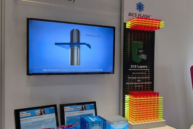
Kioxia's booth at FMS 2024 was a busy one with multiple technology demonstrations keeping visitors occupied. A walk-through of the BiCS 8 manufacturing process was the first to grab my attention. Kioxia and Western Digital announced the sampling of BiCS 8 in March 2023. We had touched briefly upon its CMOS Bonded Array (CBA) scheme in our coverage of Kioxial's 2Tb QLC NAND device and coverage of Western Digital's 128 TB QLC enterprise SSD proof-of-concept demonstration. At Kioxia's booth, we got more insights.
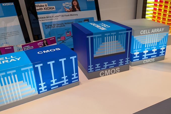
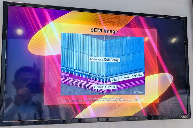
Traditionally, fabrication of flash chips involved placement of the associate logic circuitry (CMOS process) around the periphery of the flash array. The process then moved on to putting the CMOS under the cell array, but the wafer development process was serialized with the CMOS logic getting fabricated first followed by the cell array on top. However, this has some challenges because the cell array requires a high-temperature processing step to ensure higher reliability that can be detrimental to the health of the CMOS logic. Thanks to recent advancements in wafer bonding techniques, the new CBA process allows the CMOS wafer and cell array wafer to be processed independently in parallel and then pieced together, as shown in the models above.
The BiCS 8 3D NAND incorporates 218 layers, compared to 112 layers in BiCS 5 and 162 layers in BiCS 6. The company decided to skip over BiCS 7 (or, rather, it was probably a short-lived generation meant as an internal test vehicle). The generation retains the four-plane charge trap structure of BiCS 6. In its TLC avatar, it is available as a 1 Tbit device. The QLC version is available in two capacities - 1 Tbit and 2 Tbit.
Kioxia also noted that while the number of layers (218) doesn't compare favorably with the latest layer counts from the competition, its lateral scaling / cell shrinkage has enabled it to be competitive in terms of bit density as well as operating speeds (3200 MT/s). For reference, the latest shipping NAND from Micron - the G9 - has 276 layers with a bit density in TLC mode of 21 Gbit/mm2, and operates at up to 3600 MT/s. However, its 232L NAND operates only up to 2400 MT/s and has a bit density of 14.6 Gbit/mm2.
It must be noted that the CBA hybrid bonding process has advantages over the current processes used by other vendors - including Micron's CMOS under array (CuA) and SK hynix's 4D PUC (periphery-under-chip) developed in the late 2010s. It is expected that other NAND vendors will also move eventually to some variant of the hybrid bonding scheme used by Kioxia.
Storage
![The NVIDIA GTC 2024 Keynote Live Blog (Starts at 1:00pm PT/20:00 UTC) <p>We're here in sunny San Jose California for the return of an event that's been a long-time coming: NVIDIA's in-person GTC. The Spring 2024 event, NVIDIA's marquee event for the year, promises to be a big one for NVIDIA, as the company is due to deliver updates on its all-important datacenter accelerator products – the successor to the GH100 GPU and its Hopper architecture – along with NVIDIA's other professional/enterprise hardware, networking gear, and, of course, a slew of software stack updates.</p>
<p>In the 5 years since NVIDIA was last able to hold a Spring GTC in person, a great deal has changed for the company. They're now the third biggest company in the world, thanks to explosive sales growth (and even further growth expectations) due in large part to the combination of GPT-3/4 and other transformer models, and NVIDIA's transformer-optimized H100 accelerator. As a result, NVIDIA is riding high in Silicon Valley, but to keep doing so they also will need to deliver the next big thing to push the envelope on performance, and keep a number of hungry competitors off their turf.</p>
<p>Headlining today's keynote is, of course, NVIDIA CEO Jensen Huang, whose kick-off address has finally outgrown the San Jose Convention Center. As a result, Huang is filling up the local SAP Center arena instead. Suffice it to say, it's a bigger venue for a bigger audience for a [i]much[/i] bigger company.</p>
<p>So come join the AnandTech crew for our live blog coverage of NVIDIA's biggest enterprise keynote in years. The presentation kicks off at 1pm Pacific, 4pm Eastern, 20:00 UTC.</p>
Live Blog](https://4.bp.blogspot.com/-O3EpVMWcoKw/WxY6-6I4--I/AAAAAAAAB2s/KzC0FqUQtkMdw7VzT6oOR_8vbZO6EJc-ACK4BGAYYCw/w680/nth.png)

TSMC: Performance and Yields of 2nm on Track, Mass Production To Start In 2025 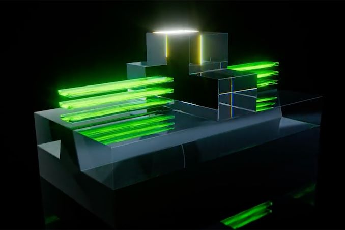
In addition to revealing its roadmap and plans concerning its current leading-edge process technologies, TSMC also shared progress of its N2 node as part of its Symposiums 2024. The company's first 2nm-class fabrication node, and predominantly featuring gate-all-around transistors, according to TSMC N2 has almost achieved its target performance and yield goals, which places it on track to enter high-volume manufacturing in the second half of 2025.
TSMC states that 'N2 development is well on track and N2P is next.' In particular, gate-all-around nanosheet devices currently achieve over 90% of their expected performance, whereas yields of 256 Mb SRAM (32 MB) devices already exceeds 80%, depending on the batch. All of this for a node that is over a year away from mass production.
Meanwhile, average yield of a 256 Mb SRAM was around 70% as of March, 2024, up from around 35% in April, 2023. Device performance has also been improving with higher frequencies being achieved while keeping power consumption in check.
Chip designer interest towards TSMC's first 2nm-class gate-all-around nanosheet transistor-based technology is significant, too. The number of new tape-outs (NTOs) in the first year of N2 is over two-times higher than it was for N5. Though with that said, given TSMC's close working relationship with a handful of high-volume vendors – most notably Appe – NTOs can be a very misleading figure since the first year of a new node at TSMC is capacity constrained, and consequently the bulk of that capacity goes to TSMC's priority partners.
Meanwhile, there were considerably more N5 tapeouts in its second year (some where N5P, of course) and N2 promises to have 2.6X more NTOs in its second year. So the node indeed looks quite promising. In fact, based on TSMC's slides (which we're unfortunately not able to republish), N2 is more popular than N3 in terms of NTOs both in the first and the second years of existence.
When it comes to the second year of N2, in the second half of 2026 TSMC plans to roll out its N2P technology, which promises additional performance and power benefits. N2P is expected to improve frequency by 15% - 20%, reduce power consumption by 30% - 40%, and increase chip density by over 1.15 times compared to N3E, significant benefits to move to all-new GAA nanosheet transistors.
Finally, for those companies that need the best in performance, power, and density, TSMC is poised to offer their A16 process in 2026. That node will also bring in backside power delivery, which will add costs, but is expected to greatly improve performance efficiency and scaling.
Semiconductors

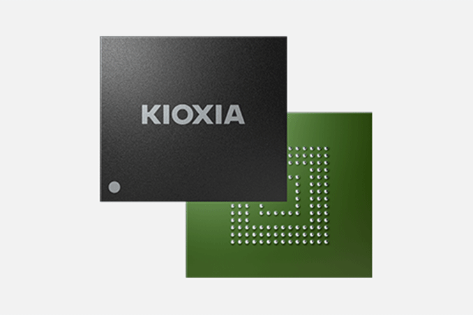
Kioxia Details BiCS 8 NAND at FMS 2024: 218 Layers With Superior Scaling
Kioxia's booth at FMS 2024 was a busy one with multiple technology demonstrations keeping visitors occupied. A walk-through of the BiCS 8 manufacturing process was the first to grab my attention. Kioxia and Western Digital announced the sampling of BiCS 8 in March 2023. We had touched briefly upon its CMOS Bonded Array (CBA) scheme in our coverage of Kioxial's 2Tb QLC NAND device and coverage of Western Digital's 128 TB QLC enterprise SSD proof-of-concept demonstration. At Kioxia's booth, we got more insights.
Traditionally, fabrication of flash chips involved placement of the associate logic circuitry (CMOS process) around the periphery of the flash array. The process then moved on to putting the CMOS under the cell array, but the wafer development process was serialized with the CMOS logic getting fabricated first followed by the cell array on top. However, this has some challenges because the cell array requires a high-temperature processing step to ensure higher reliability that can be detrimental to the health of the CMOS logic. Thanks to recent advancements in wafer bonding techniques, the new CBA process allows the CMOS wafer and cell array wafer to be processed independently in parallel and then pieced together, as shown in the models above.
The BiCS 8 3D NAND incorporates 218 layers, compared to 112 layers in BiCS 5 and 162 layers in BiCS 6. The company decided to skip over BiCS 7 (or, rather, it was probably a short-lived generation meant as an internal test vehicle). The generation retains the four-plane charge trap structure of BiCS 6. In its TLC avatar, it is available as a 1 Tbit device. The QLC version is available in two capacities - 1 Tbit and 2 Tbit.
Kioxia also noted that while the number of layers (218) doesn't compare favorably with the latest layer counts from the competition, its lateral scaling / cell shrinkage has enabled it to be competitive in terms of bit density as well as operating speeds (3200 MT/s). For reference, the latest shipping NAND from Micron - the G9 - has 276 layers with a bit density in TLC mode of 21 Gbit/mm2, and operates at up to 3600 MT/s. However, its 232L NAND operates only up to 2400 MT/s and has a bit density of 14.6 Gbit/mm2.
It must be noted that the CBA hybrid bonding process has advantages over the current processes used by other vendors - including Micron's CMOS under array (CuA) and SK hynix's 4D PUC (periphery-under-chip) developed in the late 2010s. It is expected that other NAND vendors will also move eventually to some variant of the hybrid bonding scheme used by Kioxia.
Storage
TSMC: Performance and Yields of 2nm on Track, Mass Production To Start In 2025
In addition to revealing its roadmap and plans concerning its current leading-edge process technologies, TSMC also shared progress of its N2 node as part of its Symposiums 2024. The company's first 2nm-class fabrication node, and predominantly featuring gate-all-around transistors, according to TSMC N2 has almost achieved its target performance and yield goals, which places it on track to enter high-volume manufacturing in the second half of 2025.
TSMC states that 'N2 development is well on track and N2P is next.' In particular, gate-all-around nanosheet devices currently achieve over 90% of their expected performance, whereas yields of 256 Mb SRAM (32 MB) devices already exceeds 80%, depending on the batch. All of this for a node that is over a year away from mass production.
Meanwhile, average yield of a 256 Mb SRAM was around 70% as of March, 2024, up from around 35% in April, 2023. Device performance has also been improving with higher frequencies being achieved while keeping power consumption in check.
Chip designer interest towards TSMC's first 2nm-class gate-all-around nanosheet transistor-based technology is significant, too. The number of new tape-outs (NTOs) in the first year of N2 is over two-times higher than it was for N5. Though with that said, given TSMC's close working relationship with a handful of high-volume vendors – most notably Appe – NTOs can be a very misleading figure since the first year of a new node at TSMC is capacity constrained, and consequently the bulk of that capacity goes to TSMC's priority partners.
Meanwhile, there were considerably more N5 tapeouts in its second year (some where N5P, of course) and N2 promises to have 2.6X more NTOs in its second year. So the node indeed looks quite promising. In fact, based on TSMC's slides (which we're unfortunately not able to republish), N2 is more popular than N3 in terms of NTOs both in the first and the second years of existence.
When it comes to the second year of N2, in the second half of 2026 TSMC plans to roll out its N2P technology, which promises additional performance and power benefits. N2P is expected to improve frequency by 15% - 20%, reduce power consumption by 30% - 40%, and increase chip density by over 1.15 times compared to N3E, significant benefits to move to all-new GAA nanosheet transistors.
Finally, for those companies that need the best in performance, power, and density, TSMC is poised to offer their A16 process in 2026. That node will also bring in backside power delivery, which will add costs, but is expected to greatly improve performance efficiency and scaling.
Semiconductors


Realtek Outlines SSD Controller Roadmap: High-End PCIe 5.0 x4 Platform in the Works 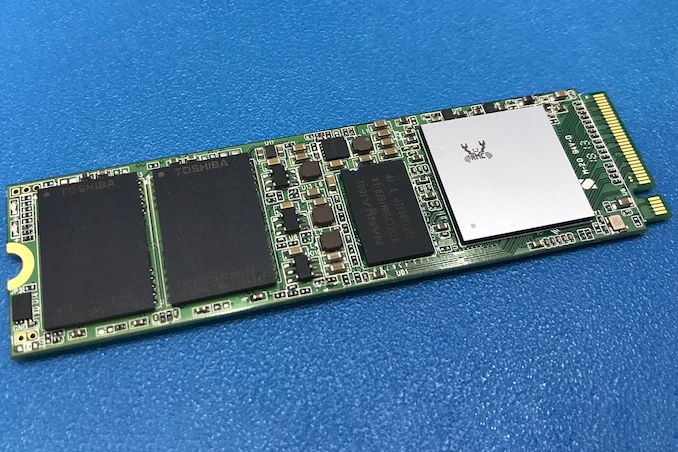
While Realtek is best known in the enthusiast space for for its peripheral controllers such as audio codecs and network controllers, the company also has a small-but-respectable SSD controller business that tends to fly under the radar due to its focus on entry-level and mainstream drives. But Realtek's stature in the SSD space is on the rise, as the company is not only planning new PCIe Gen5 SSD controllers, but also their first high-end, DRAM-equipped SSD controller.
For this year's Computex trade show, Realtek laid out a new SSD controller roadmap that calls for the company to release a trio of new SSD controllers over the next couple of years. First up is a new four-channel entry-level PCIe 4.0 controller, the RTS5776DL, which will be joined a bit later by a PCIe 5.0 variant, the RTS5781DL. But most interesting on Realtek's new roadmap is the final chip being planned: the eight-channel, DRAM-equipped RTS5782, which would be the company's first high-end SSD controller, capable of hitting sequential read rates as high as 14GB/second.
| Realtek NVMe SSD Controller Comparison | |||||||||
| RTS5782 | RTS5781DL | RTS5776DL | RTS5772DL | RTS5766DL | |||||
| Market Segment | High-End | Mainstream | Entry-Level | ||||||
| Error Correction | 4K LDPC | 2K LDPC | |||||||
| DRAM | DDR4, LPDDR4(X) | No | No | No | No | ||||
| Host Interface | PCIe 5.0 x4 | PCIe 5.0 x4 | PCIe 4.0 x4 | PCIe 4.0 x4 | PCIe 3.0 x4 | ||||
| NVMe Version | NVMe 2.0 | NVMe 2.0 | NVMe 2.0 | NVMe 1.4 | NVMe 1.4 | ||||
| NAND Channels, Interface Speed | 8 ch, 3600 MT/s |
4 ch, 3600 MT/s |
4 ch, 3600 MT/s |
8 ch, 1600 MT/s |
4 ch, 1200 MT/s |
||||
| Sequential Read | 14 GB/s | 10 GB/s | 7.4 GB/s | 6 GB/s | 3.2 GB/s | ||||
| Sequential Write | 12 GB/s | 10 GB/s | 7.4 GB/s | 6 GB/s | 2.2 GB/s | ||||
| 4KB Random Read IOPS | 2500k | 1400k | 1200k | - | - | ||||
| 4KB Random Write IOPS | 2500k | 1400k | 1200k | - | - | ||||
Diving a bit deeper into Realtek's roadmap, the RTS5776DL is traditional DRAM-less PCIe Gen4 x4 controller with four NAND chann... SSDs



Lorem Ipsum is simply dummy text of the printing and typesetting industry. Lorem Ipsum has been the industry's.
Kioxia Details BiCS 8 NAND at FMS 2024: 218 Layers With Superior Scaling
Kioxia's booth at FMS 2024 was a busy one with multiple technology demonstrations keeping visitors occupied. A walk-through of the BiCS 8 manufacturing process was the first to grab my attention. Kioxia and Western Digital announced the sampling of BiCS 8 in March 2023. We had touched briefly upon its CMOS Bonded Array (CBA) scheme in our coverage of Kioxial's 2Tb QLC NAND device and coverage of Western Digital's 128 TB QLC enterprise SSD proof-of-concept demonstration. At Kioxia's booth, we got more insights.
Traditionally, fabrication of flash chips involved placement of the associate logic circuitry (CMOS process) around the periphery of the flash array. The process then moved on to putting the CMOS under the cell array, but the wafer development process was serialized with the CMOS logic getting fabricated first followed by the cell array on top. However, this has some challenges because the cell array requires a high-temperature processing step to ensure higher reliability that can be detrimental to the health of the CMOS logic. Thanks to recent advancements in wafer bonding techniques, the new CBA process allows the CMOS wafer and cell array wafer to be processed independently in parallel and then pieced together, as shown in the models above.
The BiCS 8 3D NAND incorporates 218 layers, compared to 112 layers in BiCS 5 and 162 layers in BiCS 6. The company decided to skip over BiCS 7 (or, rather, it was probably a short-lived generation meant as an internal test vehicle). The generation retains the four-plane charge trap structure of BiCS 6. In its TLC avatar, it is available as a 1 Tbit device. The QLC version is available in two capacities - 1 Tbit and 2 Tbit.
Kioxia also noted that while the number of layers (218) doesn't compare favorably with the latest layer counts from the competition, its lateral scaling / cell shrinkage has enabled it to be competitive in terms of bit density as well as operating speeds (3200 MT/s). For reference, the latest shipping NAND from Micron - the G9 - has 276 layers with a bit density in TLC mode of 21 Gbit/mm2, and operates at up to 3600 MT/s. However, its 232L NAND operates only up to 2400 MT/s and has a bit density of 14.6 Gbit/mm2.
It must be noted that the CBA hybrid bonding process has advantages over the current processes used by other vendors - including Micron's CMOS under array (CuA) and SK hynix's 4D PUC (periphery-under-chip) developed in the late 2010s. It is expected that other NAND vendors will also move eventually to some variant of the hybrid bonding scheme used by Kioxia.
Storage
TSMC: Performance and Yields of 2nm on Track, Mass Production To Start In 2025
In addition to revealing its roadmap and plans concerning its current leading-edge process technologies, TSMC also shared progress of its N2 node as part of its Symposiums 2024. The company's first 2nm-class fabrication node, and predominantly featuring gate-all-around transistors, according to TSMC N2 has almost achieved its target performance and yield goals, which places it on track to enter high-volume manufacturing in the second half of 2025.
TSMC states that 'N2 development is well on track and N2P is next.' In particular, gate-all-around nanosheet devices currently achieve over 90% of their expected performance, whereas yields of 256 Mb SRAM (32 MB) devices already exceeds 80%, depending on the batch. All of this for a node that is over a year away from mass production.
Meanwhile, average yield of a 256 Mb SRAM was around 70% as of March, 2024, up from around 35% in April, 2023. Device performance has also been improving with higher frequencies being achieved while keeping power consumption in check.
Chip designer interest towards TSMC's first 2nm-class gate-all-around nanosheet transistor-based technology is significant, too. The number of new tape-outs (NTOs) in the first year of N2 is over two-times higher than it was for N5. Though with that said, given TSMC's close working relationship with a handful of high-volume vendors – most notably Appe – NTOs can be a very misleading figure since the first year of a new node at TSMC is capacity constrained, and consequently the bulk of that capacity goes to TSMC's priority partners.
Meanwhile, there were considerably more N5 tapeouts in its second year (some where N5P, of course) and N2 promises to have 2.6X more NTOs in its second year. So the node indeed looks quite promising. In fact, based on TSMC's slides (which we're unfortunately not able to republish), N2 is more popular than N3 in terms of NTOs both in the first and the second years of existence.
When it comes to the second year of N2, in the second half of 2026 TSMC plans to roll out its N2P technology, which promises additional performance and power benefits. N2P is expected to improve frequency by 15% - 20%, reduce power consumption by 30% - 40%, and increase chip density by over 1.15 times compared to N3E, significant benefits to move to all-new GAA nanosheet transistors.
Finally, for those companies that need the best in performance, power, and density, TSMC is poised to offer their A16 process in 2026. That node will also bring in backside power delivery, which will add costs, but is expected to greatly improve performance efficiency and scaling.
Semiconductors
0 Comments