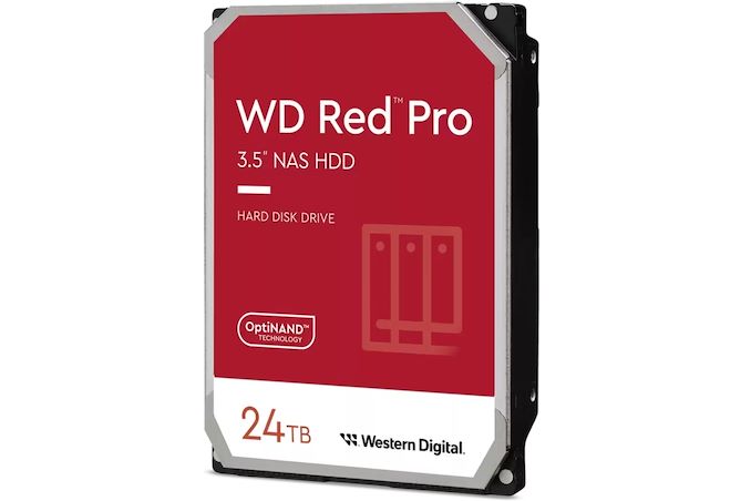
Western Digital Ships 24TB Red Pro Hard Drive For NASes [UPDATED] <p align="center"><a href="https://www.anandtech.com/show/21329/western-digital-ships-24tb-hdd"><img src="https://images.anandtech.com/doci/21329/wd-western-digital-wd-red-hdd-678_575px.jpg" alt="" /></a></p><p><p>Nowadays highest-capacity hard drives are typically aimed at cloud service providers (CSPs) and enterprises, but this does not mean that creative professionals or regular users do not need them. To cater to demands of more regular consumers, Western Digital has started shipments of its <a href="https://www.westerndigital.com/products/internal-drives/wd-red-pro-sata-hdd?sku=WD240KFGX">Red Pro 24 TB HDDs,</a> which are aimed at high-end NAS use for creative professionals with significant storage requirements.</p>
<p><a href="https://documents.westerndigital.com/content/dam/doc-library/en_us/assets/public/western-digital/product/internal-drives/wd-red-pro-hdd/product-brief-western-digital-wd-red-pro-hdd.pdf">Western Digital's Red Pro 24 TB hard drives</a> come approximately 20 months after their <a href="https://www.anandtech.com/show/17501/western-digital-22tb-wd-gold-red-pro-and-purple-hdds-hit-retail">22 TB model hit retail in 2022</a>, offering an incremental improvement to WD's highest-capacity NAS and consumer hard drive offering. The platform uses conventional magnetic recording (CMR), feature a 7200 RPM rotating speed, are equipped with a 512 MB cache, and use OptiNAND technology to improve reliability as well as optimize performance and power consumption. The HDDs are rated for an up to 287 MB/s media to cache transfer rate, which makes them some of the fastest hard drives around (albeit, still a bit slower compared to CSP and enterprise-oriented HDDs).</p>
<p style="text-align: center;"><a href="https://www.anandtech.com/show/21329/western-digital-ships-24tb-hdd"><img alt="" src="https://images.anandtech.com/doci/21329/wd-western-digital-wd-red-hdd-s_575px.jpg" /></a></p>
<p>Just like other high-end network-attached storage-aimed HDDs, the <a href="https://www.westerndigital.com/products/internal-drives/wd-red-pro-sata-hdd?sku=WD240KFGX">Red Pro 24 TB</a> hard drives use helium-filled platforms that are very similar to those designed for enterprise drives. Consequently, the Red Pro 24 TB HDD are equipped with rotation vibration sensors to anticipate and proactively counteract disturbances caused by increased vibration and multi-axis shock sensors to detect subtle shock events and automatically offset them with dynamic fly height technology to ensure that heads to not scratch disks.</p>
<p><strong>UPDATE 4/2/2024: </strong>Western Digital has notified us that WD Red Pro fully support ArmorCache capability, even though it is not listed in datasheets.</p>
<p><s>What these drives lack compared</s> Apparently, just like <a href="https://documents.westerndigital.com/content/dam/doc-library/en_us/assets/public/western-digital/product/internal-drives/wd-gold/product-brief-wd-gold-hdd.pdf">WD Gold</a> and Ultraster 22 TB and 24 TB drives for enterprises and cloud datacenters, WD Red Pro HDDs fully support the ArmorCache feature that provides protection against power loss when write-cache is enabled (WCE mode) and enhances performance when write-cache is disabled (WCD mode).</p>
<p>On the reliability side of matters, Western Digital's Red Pro 24 TB HDDs are designed for 24/7 operation in vibrating environments, such as enterprise-grade NAS with loads of bays, and are rated for up to 550 TB/year workloads as well as up to 600,000 load/unload cycles, which is in line with what Western Digital's WD Gold and Ultrastar hard drives offer.</p>
<p>As for power consumption, the WD Red Pro 24 TB consumes up to 6.4W during read and write operations, up to 3.9W in idle mode, and up to 1.2W in standby/sleep mode.</p>
<p>Western Digital's Red Pro 24 TB (WD240KFGX) HDDs are now shipping to resellers as well as NAS makers, and are slated to be available shortly. Expect these hard drives to be slightly cheaper than the WD Gold 24 TB model.</p>
</p> Storage
Western Digital Ships 24TB Red Pro Hard Drive For NASes [UPDATED]
Nowadays highest-capacity hard drives are typically aimed at cloud service providers (CSPs) and enterprises, but this does not mean that creative professionals or regular users do not need them. To cater to demands of more regular consumers, Western Digital has started shipments of its Red Pro 24 TB HDDs, which are aimed at high-end NAS use for creative professionals with significant storage requirements.
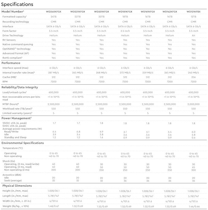
Western Digital's Red Pro 24 TB hard drives come approximately 20 months after their 22 TB model hit retail in 2022, offering an incremental improvement to WD's highest-capacity NAS and consumer hard drive offering. The platform uses conventional magnetic recording (CMR), feature a 7200 RPM rotating speed, are equipped with a 512 MB cache, and use OptiNAND technology to improve reliability as well as optimize performance and power consumption. The HDDs are rated for an up to 287 MB/s media to cache transfer rate, which makes them some of the fastest hard drives around (albeit, still a bit slower compared to CSP and enterprise-oriented HDDs).
Just like other high-end network-attached storage-aimed HDDs, the Red Pro 24 TB hard drives use helium-filled platforms that are very similar to those designed for enterprise drives. Consequently, the Red Pro 24 TB HDD are equipped with rotation vibration sensors to anticipate and proactively counteract disturbances caused by increased vibration and multi-axis shock sensors to detect subtle shock events and automatically offset them with dynamic fly height technology to ensure that heads to not scratch disks.
UPDATE 4/2/2024: Western Digital has notified us that WD Red Pro fully support ArmorCache capability, even though it is not listed in datasheets.
What these drives lack compared Apparently, just like WD Gold and Ultraster 22 TB and 24 TB drives for enterprises and cloud datacenters, WD Red Pro HDDs fully support the ArmorCache feature that provides protection against power loss when write-cache is enabled (WCE mode) and enhances performance when write-cache is disabled (WCD mode).
On the reliability side of matters, Western Digital's Red Pro 24 TB HDDs are designed for 24/7 operation in vibrating environments, such as enterprise-grade NAS with loads of bays, and are rated for up to 550 TB/year workloads as well as up to 600,000 load/unload cycles, which is in line with what Western Digital's WD Gold and Ultrastar hard drives offer.
As for power consumption, the WD Red Pro 24 TB consumes up to 6.4W during read and write operations, up to 3.9W in idle mode, and up to 1.2W in standby/sleep mode.
Western Digital's Red Pro 24 TB (WD240KFGX) HDDs are now shipping to resellers as well as NAS makers, and are slated to be available shortly. Expect these hard drives to be slightly cheaper than the WD Gold 24 TB model.


 and enterprises, but this does not mean that creative professionals or regular users do not need them. To cater to demands of more regular consumers, Western Digital has started shipments of its <a href="https://www.westerndigital.com/products/internal-drives/wd-red-pro-sata-hdd?sku=WD240KFGX">Red Pro 24 TB HDDs,</a> which are aimed at high-end NAS use for creative professionals with significant storage requirements.</p>
<p><a href="https://documents.westerndigital.com/content/dam/doc-library/en_us/assets/public/western-digital/product/internal-drives/wd-red-pro-hdd/product-brief-western-digital-wd-red-pro-hdd.pdf">Western Digital's Red Pro 24 TB hard drives</a> come approximately 20 months after their <a href="https://www.anandtech.com/show/17501/western-digital-22tb-wd-gold-red-pro-and-purple-hdds-hit-retail">22 TB model hit retail in 2022</a>, offering an incremental improvement to WD's highest-capacity NAS and consumer hard drive offering. The platform uses conventional magnetic recording (CMR), feature a 7200 RPM rotating speed, are equipped with a 512 MB cache, and use OptiNAND technology to improve reliability as well as optimize performance and power consumption. The HDDs are rated for an up to 287 MB/s media to cache transfer rate, which makes them some of the fastest hard drives around (albeit, still a bit slower compared to CSP and enterprise-oriented HDDs).</p>
<p style="text-align: center;"><a href="https://www.anandtech.com/show/21329/western-digital-ships-24tb-hdd"><img alt="" src="https://images.anandtech.com/doci/21329/wd-western-digital-wd-red-hdd-s_575px.jpg" /></a></p>
<p>Just like other high-end network-attached storage-aimed HDDs, the <a href="https://www.westerndigital.com/products/internal-drives/wd-red-pro-sata-hdd?sku=WD240KFGX">Red Pro 24 TB</a> hard drives use helium-filled platforms that are very similar to those designed for enterprise drives. Consequently, the Red Pro 24 TB HDD are equipped with rotation vibration sensors to anticipate and proactively counteract disturbances caused by increased vibration and multi-axis shock sensors to detect subtle shock events and automatically offset them with dynamic fly height technology to ensure that heads to not scratch disks.</p>
<p><strong>UPDATE 4/2/2024: </strong>Western Digital has notified us that WD Red Pro fully support ArmorCache capability, even though it is not listed in datasheets.</p>
<p><s>What these drives lack compared</s> Apparently, just like <a href="https://documents.westerndigital.com/content/dam/doc-library/en_us/assets/public/western-digital/product/internal-drives/wd-gold/product-brief-wd-gold-hdd.pdf">WD Gold</a> and Ultraster 22 TB and 24 TB drives for enterprises and cloud datacenters, WD Red Pro HDDs fully support the ArmorCache feature that provides protection against power loss when write-cache is enabled (WCE mode) and enhances performance when write-cache is disabled (WCD mode).</p>
<p>On the reliability side of matters, Western Digital's Red Pro 24 TB HDDs are designed for 24/7 operation in vibrating environments, such as enterprise-grade NAS with loads of bays, and are rated for up to 550 TB/year workloads as well as up to 600,000 load/unload cycles, which is in line with what Western Digital's WD Gold and Ultrastar hard drives offer.</p>
<p>As for power consumption, the WD Red Pro 24 TB consumes up to 6.4W during read and write operations, up to 3.9W in idle mode, and up to 1.2W in standby/sleep mode.</p>
<p>Western Digital's Red Pro 24 TB (WD240KFGX) HDDs are now shipping to resellers as well as NAS makers, and are slated to be available shortly. Expect these hard drives to be slightly cheaper than the WD Gold 24 TB model.</p>
</p> Storage)
 and enterprises, but this does not mean that creative professionals or regular users do not need them. To cater to demands of more regular consumers, Western Digital has started shipments of its <a href="https://www.westerndigital.com/products/internal-drives/wd-red-pro-sata-hdd?sku=WD240KFGX">Red Pro 24 TB HDDs,</a> which are aimed at high-end NAS use for creative professionals with significant storage requirements.</p>
<p><a href="https://documents.westerndigital.com/content/dam/doc-library/en_us/assets/public/western-digital/product/internal-drives/wd-red-pro-hdd/product-brief-western-digital-wd-red-pro-hdd.pdf">Western Digital's Red Pro 24 TB hard drives</a> come approximately 20 months after their <a href="https://www.anandtech.com/show/17501/western-digital-22tb-wd-gold-red-pro-and-purple-hdds-hit-retail">22 TB model hit retail in 2022</a>, offering an incremental improvement to WD's highest-capacity NAS and consumer hard drive offering. The platform uses conventional magnetic recording (CMR), feature a 7200 RPM rotating speed, are equipped with a 512 MB cache, and use OptiNAND technology to improve reliability as well as optimize performance and power consumption. The HDDs are rated for an up to 287 MB/s media to cache transfer rate, which makes them some of the fastest hard drives around (albeit, still a bit slower compared to CSP and enterprise-oriented HDDs).</p>
<p style="text-align: center;"><a href="https://www.anandtech.com/show/21329/western-digital-ships-24tb-hdd"><img alt="" src="https://images.anandtech.com/doci/21329/wd-western-digital-wd-red-hdd-s_575px.jpg" /></a></p>
<p>Just like other high-end network-attached storage-aimed HDDs, the <a href="https://www.westerndigital.com/products/internal-drives/wd-red-pro-sata-hdd?sku=WD240KFGX">Red Pro 24 TB</a> hard drives use helium-filled platforms that are very similar to those designed for enterprise drives. Consequently, the Red Pro 24 TB HDD are equipped with rotation vibration sensors to anticipate and proactively counteract disturbances caused by increased vibration and multi-axis shock sensors to detect subtle shock events and automatically offset them with dynamic fly height technology to ensure that heads to not scratch disks.</p>
<p><strong>UPDATE 4/2/2024: </strong>Western Digital has notified us that WD Red Pro fully support ArmorCache capability, even though it is not listed in datasheets.</p>
<p><s>What these drives lack compared</s> Apparently, just like <a href="https://documents.westerndigital.com/content/dam/doc-library/en_us/assets/public/western-digital/product/internal-drives/wd-gold/product-brief-wd-gold-hdd.pdf">WD Gold</a> and Ultraster 22 TB and 24 TB drives for enterprises and cloud datacenters, WD Red Pro HDDs fully support the ArmorCache feature that provides protection against power loss when write-cache is enabled (WCE mode) and enhances performance when write-cache is disabled (WCD mode).</p>
<p>On the reliability side of matters, Western Digital's Red Pro 24 TB HDDs are designed for 24/7 operation in vibrating environments, such as enterprise-grade NAS with loads of bays, and are rated for up to 550 TB/year workloads as well as up to 600,000 load/unload cycles, which is in line with what Western Digital's WD Gold and Ultrastar hard drives offer.</p>
<p>As for power consumption, the WD Red Pro 24 TB consumes up to 6.4W during read and write operations, up to 3.9W in idle mode, and up to 1.2W in standby/sleep mode.</p>
<p>Western Digital's Red Pro 24 TB (WD240KFGX) HDDs are now shipping to resellers as well as NAS makers, and are slated to be available shortly. Expect these hard drives to be slightly cheaper than the WD Gold 24 TB model.</p>
</p> Storage | https://compbuddey.blogspot.com/2024/04/western-digital-ships-24tb-red-pro-hard_3.html)
 and enterprises, but this does not mean that creative professionals or regular users do not need them. To cater to demands of more regular consumers, Western Digital has started shipments of its <a href="https://www.westerndigital.com/products/internal-drives/wd-red-pro-sata-hdd?sku=WD240KFGX">Red Pro 24 TB HDDs,</a> which are aimed at high-end NAS use for creative professionals with significant storage requirements.</p>
<p><a href="https://documents.westerndigital.com/content/dam/doc-library/en_us/assets/public/western-digital/product/internal-drives/wd-red-pro-hdd/product-brief-western-digital-wd-red-pro-hdd.pdf">Western Digital's Red Pro 24 TB hard drives</a> come approximately 20 months after their <a href="https://www.anandtech.com/show/17501/western-digital-22tb-wd-gold-red-pro-and-purple-hdds-hit-retail">22 TB model hit retail in 2022</a>, offering an incremental improvement to WD's highest-capacity NAS and consumer hard drive offering. The platform uses conventional magnetic recording (CMR), feature a 7200 RPM rotating speed, are equipped with a 512 MB cache, and use OptiNAND technology to improve reliability as well as optimize performance and power consumption. The HDDs are rated for an up to 287 MB/s media to cache transfer rate, which makes them some of the fastest hard drives around (albeit, still a bit slower compared to CSP and enterprise-oriented HDDs).</p>
<p style="text-align: center;"><a href="https://www.anandtech.com/show/21329/western-digital-ships-24tb-hdd"><img alt="" src="https://images.anandtech.com/doci/21329/wd-western-digital-wd-red-hdd-s_575px.jpg" /></a></p>
<p>Just like other high-end network-attached storage-aimed HDDs, the <a href="https://www.westerndigital.com/products/internal-drives/wd-red-pro-sata-hdd?sku=WD240KFGX">Red Pro 24 TB</a> hard drives use helium-filled platforms that are very similar to those designed for enterprise drives. Consequently, the Red Pro 24 TB HDD are equipped with rotation vibration sensors to anticipate and proactively counteract disturbances caused by increased vibration and multi-axis shock sensors to detect subtle shock events and automatically offset them with dynamic fly height technology to ensure that heads to not scratch disks.</p>
<p><strong>UPDATE 4/2/2024: </strong>Western Digital has notified us that WD Red Pro fully support ArmorCache capability, even though it is not listed in datasheets.</p>
<p><s>What these drives lack compared</s> Apparently, just like <a href="https://documents.westerndigital.com/content/dam/doc-library/en_us/assets/public/western-digital/product/internal-drives/wd-gold/product-brief-wd-gold-hdd.pdf">WD Gold</a> and Ultraster 22 TB and 24 TB drives for enterprises and cloud datacenters, WD Red Pro HDDs fully support the ArmorCache feature that provides protection against power loss when write-cache is enabled (WCE mode) and enhances performance when write-cache is disabled (WCD mode).</p>
<p>On the reliability side of matters, Western Digital's Red Pro 24 TB HDDs are designed for 24/7 operation in vibrating environments, such as enterprise-grade NAS with loads of bays, and are rated for up to 550 TB/year workloads as well as up to 600,000 load/unload cycles, which is in line with what Western Digital's WD Gold and Ultrastar hard drives offer.</p>
<p>As for power consumption, the WD Red Pro 24 TB consumes up to 6.4W during read and write operations, up to 3.9W in idle mode, and up to 1.2W in standby/sleep mode.</p>
<p>Western Digital's Red Pro 24 TB (WD240KFGX) HDDs are now shipping to resellers as well as NAS makers, and are slated to be available shortly. Expect these hard drives to be slightly cheaper than the WD Gold 24 TB model.</p>
</p> Storage&body=https://compbuddey.blogspot.com/2024/04/western-digital-ships-24tb-red-pro-hard_3.html)
0 Comments