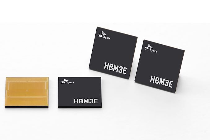

SK Hynix said that it had started volume production of its HBM3E memory and would supply it to a customer in late March. The South Korean company is the second DRAM producer to announce mass production of HBM3E, so the market of ultra-high-performance memory will have some competition, which is good for companies that plan to use HBM3E.
According to specifications, SK Hynix's HBM3E known good stack dies (KGSDs) feature data transfer rates up to 9.2 GT/s, a 1024-bit interface, and a bandwidth of 1.18 TB/s, which is massively higher than the 6.4 GT/s and 819 GB/s offered by HBM3. The company does not say whether it mass produces 8Hi 24GB HBM3E memory modules or 12Hi 36GB HBM3E devices, but it will likely begin its HBM3E ramp from lower-capacity products as they are easier to make.
We already know that SK Hynix's HBM3E stacks employ the company's advanced Mass Reflow Molded Underfill (MR-RUF) technology, which promises to reduce heat dissipation by 10%. This technology involves the use of an enhanced underfill between DRAM layers, which not only improves heat dissipation but also reduces the thickness of HBM stacks. As a result, 12-Hi HBM stacks can be constructed that are the same height as 8-Hi modules. However, this does not necessarily imply that the stacks currently in mass production are 12-Hi HBM3E stacks.
Although the memory maker does not officially confirm this, SK Hynix's 24GB HBM3E stacks will arrive just in time to address NVIDIA's Blackwell accelerator family for artificial intelligence and high-performance computing applications.
"With the success story of the HBM business and the strong partnership with customers that it has built for years, SK Hynix will cement its position as the total AI memory provider," said Sungsoo Ryu, Head of HBM business at SK Hynix. As a result, NVIDIA will have access to HBM3E memory from multiple suppliers with both Micron and SK Hynix.
Meanwhile, AMD recently confirmed that it was looking forward to expanding its Instinct MI300-series lineup for AI and HPC applications with higher-performance memory configurations, so SK Hynix's HBM3E memory could also be used for this.
DRAM

Demand for high-performance processors for AI training is skyrocketing, and consequently so is the demand for the components that go into these processors. So much so that SK hynix this week is very publicly announcing that the company's high-bandwidth memory (HBM) production capacity has already sold out for the rest of 2024, and even most of 2025 has already sold out as well.
SK hynix currently produces various types of HBM memory for customers like Amazon, AMD, Facebook, Google (Broadcom), Intel, Microsoft, and, of course, NVIDIA. The latter is an especially prolific consumer of HBM3 and HBM3E memory for its H100/H200/GH200 accelerators, as NVIDIA is also working to fill what remains an insatiable (and unmet) demand for its accelerators.
As a result, HBM memory orders, which are already placed months in advance, are now backlogging well into 2025 as chip vendors look to secure supplies of the memory stacks critical to their success.
This has made SK hynix the secnd HBM memory vendor in recent months to announce that they've sold out into 2025, following an earlier announcement from Micron regarding its HBM3E production. But of the two announcements, SK hynix's is arguably the most significant yet, as the South Korean firm's HBM production capacity is far greater than Micron's. So while things were merely "interesting" with the smallest of the Big Three memory manufacturers being sold out into 2025, things are taking a more concerning (and constrained) outlook now that SK hynix is as well.
SK hynix currently controls roughly 46% - 49% of HBM market, and its share is not expected to drop significantly in 2025, according to market tracking firm TrendForce. By contrast, Micron's share on HBM memory market is between 4% and 6%. Since HBM supply of both companies is sold out through the most of 2025, we're likely looking at a scenario where over 50% of the industry's total HBM3/HBM3E supply for the coming quarters is already sold out.
This leaves Samsung as the only member of the group not to comment on HBM demand so far. Though with memory being a highly fungible commodity product, it would be surprising if Samsung wasn't facing similar demand. And, ultimately, all of this is pointing towards the indusry entering an HBM3 memory shortage.
Separately, SK hynix said that it is sampling 12-Hi 36GB HBM3E stacks with customers and will begin volume shipments in the third quarter.
Memory
Lorem Ipsum is simply dummy text of the printing and typesetting industry. Lorem Ipsum has been the industry's.
Demand for high-performance processors for AI training is skyrocketing, and consequently so is the demand for the components that go into these processors. So much so that SK hynix this week is very publicly announcing that the company's high-bandwidth memory (HBM) production capacity has already sold out for the rest of 2024, and even most of 2025 has already sold out as well.
SK hynix currently produces various types of HBM memory for customers like Amazon, AMD, Facebook, Google (Broadcom), Intel, Microsoft, and, of course, NVIDIA. The latter is an especially prolific consumer of HBM3 and HBM3E memory for its H100/H200/GH200 accelerators, as NVIDIA is also working to fill what remains an insatiable (and unmet) demand for its accelerators.
As a result, HBM memory orders, which are already placed months in advance, are now backlogging well into 2025 as chip vendors look to secure supplies of the memory stacks critical to their success.
This has made SK hynix the secnd HBM memory vendor in recent months to announce that they've sold out into 2025, following an earlier announcement from Micron regarding its HBM3E production. But of the two announcements, SK hynix's is arguably the most significant yet, as the South Korean firm's HBM production capacity is far greater than Micron's. So while things were merely "interesting" with the smallest of the Big Three memory manufacturers being sold out into 2025, things are taking a more concerning (and constrained) outlook now that SK hynix is as well.
SK hynix currently controls roughly 46% - 49% of HBM market, and its share is not expected to drop significantly in 2025, according to market tracking firm TrendForce. By contrast, Micron's share on HBM memory market is between 4% and 6%. Since HBM supply of both companies is sold out through the most of 2025, we're likely looking at a scenario where over 50% of the industry's total HBM3/HBM3E supply for the coming quarters is already sold out.
This leaves Samsung as the only member of the group not to comment on HBM demand so far. Though with memory being a highly fungible commodity product, it would be surprising if Samsung wasn't facing similar demand. And, ultimately, all of this is pointing towards the indusry entering an HBM3 memory shortage.
Separately, SK hynix said that it is sampling 12-Hi 36GB HBM3E stacks with customers and will begin volume shipments in the third quarter.
Memory


 feature data transfer rates up to 9.2 GT/s, a 1024-bit interface, and a bandwidth of 1.18 TB/s, which is massively higher than the 6.4 GT/s and 819 GB/s offered by HBM3. The company does not say whether it mass produces 8Hi 24GB HBM3E memory modules or 12Hi 36GB HBM3E devices, but it will likely begin its HBM3E ramp from lower-capacity products as they are easier to make.</p>
<p>We already know that SK Hynix's HBM3E stacks employ the company's advanced Mass Reflow Molded Underfill (MR-RUF) technology, which promises to reduce heat dissipation by 10%. This technology involves the use of an enhanced underfill between DRAM layers, which not only improves heat dissipation but also reduces the thickness of HBM stacks. As a result, 12-Hi HBM stacks can be constructed that are the same height as 8-Hi modules. However, this does not necessarily imply that the stacks currently in mass production are 12-Hi HBM3E stacks.</p>
<p>Although the memory maker does not officially confirm this, SK Hynix's 24GB HBM3E stacks will arrive just in time to address NVIDIA's Blackwell accelerator family for artificial intelligence and high-performance computing applications.</p>
<p>"<em>With the success story of the HBM business and the strong partnership with customers that it has built for years, SK Hynix will cement its position as the total AI memory provider,</em>" said Sungsoo Ryu, Head of HBM business at SK Hynix. As a result, NVIDIA will have access to HBM3E memory from multiple suppliers with both Micron and SK Hynix.</p>
<p>Meanwhile, AMD recently confirmed that it was looking forward to expanding its Instinct MI300-series lineup for AI and HPC applications with higher-performance memory configurations, so SK Hynix's HBM3E memory could also be used for this.</p>
</p> DRAM)
 feature data transfer rates up to 9.2 GT/s, a 1024-bit interface, and a bandwidth of 1.18 TB/s, which is massively higher than the 6.4 GT/s and 819 GB/s offered by HBM3. The company does not say whether it mass produces 8Hi 24GB HBM3E memory modules or 12Hi 36GB HBM3E devices, but it will likely begin its HBM3E ramp from lower-capacity products as they are easier to make.</p>
<p>We already know that SK Hynix's HBM3E stacks employ the company's advanced Mass Reflow Molded Underfill (MR-RUF) technology, which promises to reduce heat dissipation by 10%. This technology involves the use of an enhanced underfill between DRAM layers, which not only improves heat dissipation but also reduces the thickness of HBM stacks. As a result, 12-Hi HBM stacks can be constructed that are the same height as 8-Hi modules. However, this does not necessarily imply that the stacks currently in mass production are 12-Hi HBM3E stacks.</p>
<p>Although the memory maker does not officially confirm this, SK Hynix's 24GB HBM3E stacks will arrive just in time to address NVIDIA's Blackwell accelerator family for artificial intelligence and high-performance computing applications.</p>
<p>"<em>With the success story of the HBM business and the strong partnership with customers that it has built for years, SK Hynix will cement its position as the total AI memory provider,</em>" said Sungsoo Ryu, Head of HBM business at SK Hynix. As a result, NVIDIA will have access to HBM3E memory from multiple suppliers with both Micron and SK Hynix.</p>
<p>Meanwhile, AMD recently confirmed that it was looking forward to expanding its Instinct MI300-series lineup for AI and HPC applications with higher-performance memory configurations, so SK Hynix's HBM3E memory could also be used for this.</p>
</p> DRAM | https://compbuddey.blogspot.com/2024/04/sk-hynix-starts-mass-production-of_5.html)
 feature data transfer rates up to 9.2 GT/s, a 1024-bit interface, and a bandwidth of 1.18 TB/s, which is massively higher than the 6.4 GT/s and 819 GB/s offered by HBM3. The company does not say whether it mass produces 8Hi 24GB HBM3E memory modules or 12Hi 36GB HBM3E devices, but it will likely begin its HBM3E ramp from lower-capacity products as they are easier to make.</p>
<p>We already know that SK Hynix's HBM3E stacks employ the company's advanced Mass Reflow Molded Underfill (MR-RUF) technology, which promises to reduce heat dissipation by 10%. This technology involves the use of an enhanced underfill between DRAM layers, which not only improves heat dissipation but also reduces the thickness of HBM stacks. As a result, 12-Hi HBM stacks can be constructed that are the same height as 8-Hi modules. However, this does not necessarily imply that the stacks currently in mass production are 12-Hi HBM3E stacks.</p>
<p>Although the memory maker does not officially confirm this, SK Hynix's 24GB HBM3E stacks will arrive just in time to address NVIDIA's Blackwell accelerator family for artificial intelligence and high-performance computing applications.</p>
<p>"<em>With the success story of the HBM business and the strong partnership with customers that it has built for years, SK Hynix will cement its position as the total AI memory provider,</em>" said Sungsoo Ryu, Head of HBM business at SK Hynix. As a result, NVIDIA will have access to HBM3E memory from multiple suppliers with both Micron and SK Hynix.</p>
<p>Meanwhile, AMD recently confirmed that it was looking forward to expanding its Instinct MI300-series lineup for AI and HPC applications with higher-performance memory configurations, so SK Hynix's HBM3E memory could also be used for this.</p>
</p> DRAM&body=https://compbuddey.blogspot.com/2024/04/sk-hynix-starts-mass-production-of_5.html)
0 Comments