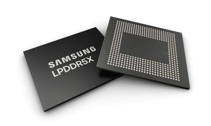
Samsung today has announced that they have developed an even faster generation of LPDDR5X memory that is set to top out at LPDDR5X-10700 speeds. The updated memory is slated to offer 25% better performance and 30% greater capacity compared to existing mobile DRAM devices from the company. The new chips also appear to be tangibly faster than Micron's LPDDR5X memory and SK hynix's LPDDR5T chips.
Samsung's forthcoming LPDDR5X devices feature a data transfer rate of 10.7 GT/s as well as maximum capacity per stack of 32 GB. This allows Samsung's clients to equip their latest smartphones or laptops with 32 GB of low-power memory using just one DRAM package, which greatly simplifies their designs. Samsung says that 32 GB of memory will be particularly beneficial for on-device AI applications.
Samsung is using its latest-generation 12nm-class DRAM process technology to make its LPDDR5X-10700 devices, which allows the company to achieve the smallest LPDDR device size in the industry, the memory maker said.
In terms of power efficiency, Samsung claims that they have integrated multiple new power-saving features into the new LPDDR5X devices. These include an optimized power variation system that adjusts energy consumption based on workload, and expanded intervals for low-power mode that extend the periods of energy saving. These innovations collectively enhance power efficiency by 25% compared to earlier versions, benefiting mobile platforms by extending battery life, the company said.
“As demand for low-power, high-performance memory increases, LPDDR DRAM is expected to expand its applications from mainly mobile to other areas that traditionally require higher performance and reliability such as PCs, accelerators, servers and automobiles,” said YongCheol Bae, Executive Vice President of Memory Product Planning of the Memory Business at Samsung Electronics. “Samsung will continue to innovate and deliver optimized products for the upcoming on-device AI era through close collaboration with customers.”
Samsung plans to initiate mass production of the 10.7 GT/s LPDDR5X DRAM in the second half of this year. This follows a series of compatibility tests with mobile application processors and device manufacturers to ensure seamless integration into future products.
DRAMAMD Quietly Launches Ryzen 7 8700F and Ryzen 5 8400F Processors AMD has recently expanded its Ryzen 8000 series by introducing the Ryzen 7 8700F and Ryzen 5 8400F processors. Initially launched in China, these chips were added to AMD's global website, signaling they are available worldwide, apparently from April 1st. Built from the recent Zen 4-based Phoenix APUs using the TSMC 4nm node as their Zen 4 mobile chips, these new CPUs lack integrated graphics. However, the Ryzen 7 8700F does include the integrated Ryzen AI NPU for added capabilities in a world currently dominated by AI and moving it directly into the PC. The company's decision to announce these chips in China aligns with its strategy to offer Ryzen solutions at every price point in the market. Although AMD didn't initially disclose the full specifications of these F-series models, and we did reach out to the company to ask about them, they refused to discuss them with us. Their listing on the website has now been updated with a complete list of specifications and features, with everything but the price mentioned. AMD Ryzen 8000G vs. Ryzen 8000F Series (Desktop) Zen 4 (Phoenix) AnandTech Cores/Threads Base Freq Turbo Freq GPU GPU Freq Ryzen AI (NPU) L3 Cache (MB) TDP MSRP Ryzen 7 Ryzen 7 8700G 8/16 4200 5100 R780M 12 CUs 2900 Y 16 65W $329 Ryzen 7 8700F 8/16 4100 5000 - - Y 16 65W ? Ryzen 5 Ryzen 5 8600G 6/12 4300 5000 R760M 8 CUs 2800 Y 16 65W $229 Ryzen 5 8400F 6/12 4200 4700 - - N 16 65W ? The Ryzen 7 8700F features an 8C/16T design, with 16MB of L3 cache and the same 65W TDP as the Ryzen 7 8700G. Although the base clock speed is 4.1 GHz, it boosts to 5.0 GHz; this is 100 MHz less on both base/boost clocks than the 8700G. Meanwhile, the Ryzen 5 8400F is a slightly scaled-down version of the Ryzen 8600G APU, with 6C/12, 16MB of L3 cache, and again has a 100 MHz reduction to base clocks compared to the 8600G. Unlike the Ryzen 5 8400F, the Ryzen 7 8700F keeps AMD's Ryzen AI NPU, adding additional capability for generative AI. The Ryzen 5 8400F can boost up to 4.7 GHz, 300 MHz slower than the Ryzen 5 8600G. AMD also allows overclocking for these new F-series chips, which means users could potentially boost the performance of these processors to match their G-series equivalents. Pricing details are still pending, but to remain competitive, AMD will likely need to price these CPUs below the 8700G and 8600G, as well as the Ryzen 7 7700 and Ryzen 5 7600. These CPUs offer, albeit very limited, integrated graphics and have double the L3 cache capacity, along with higher boost clocks than the 8000F series chips, so pricing is something to consider whenever pricing becomes available. CPUs
Samsung To Receive $6.4 Billion Under CHIPS Act to Build $40 Billion Fab in Texas Samsung Electronics this week was awarded up to $6.4 billion from the U.S. government under the CHIPS and Science Act to build its new fab complex in Taylor, Texas. This is the third major award under the act in the last month, with all three leading-edge fabs – Intel, TSMC, and now Samsung – receiving multi-billion dollar funding packages under the domestic chip production program. Overall, the final price tag on Samsung's new fab complex is expected to reach $40 billion by the time it's completed later this decade. Samsung's CHIPS Act funding was announced during a celebratory event attended by U.S. Secretary of Commerce Gina Raimondo and Samsung Semiconductor chief executive Kye Hyun Kyung. During the event, Kyung outlined the strategic goals of the expansion, emphasizing that the additional funding will not only increase production capacity but also strengthen the entire local semiconductor ecosystem. Samsung plans to equip its fab near Taylor, Texas, with the latest wafer fab tools to produce advanced chips. The Financial Times reports that Samsung aims to produce semiconductors on its 2nm-class process technology starting 2026, though for now this is unofficial information. "I am pleased to announce a preliminary agreement between Samsung and the Department of Commerce to bring Samsung's advanced semiconductor manufacturing and research and development to Texas," said Joe Biden, the U.S. president, in a statement. "This announcement will unleash over $40 billion in investment from Samsung, and cement central Texas's role as a state-of-the-art semiconductor ecosystem, creating at least 21,500 jobs and leveraging up to $40 million in CHIPS funding to train and develop the local workforce. These facilities will support the production of some of the most powerful chips in the world, which are essential to advanced technologies like artificial intelligence and will bolster U.S. national security." Samsung has been a significant contributor to the Texas economy for decades, starting chip manufacturing in the U.S. in 1996. With previous investments totaling $18 billion in its Austin operations, Samsung's expansion into Taylor with an additional investment of at least $17 billion underscores its role as one of the largest foreign direct investors in U.S. history. The total expected investment in the new fab surpasses $40 billion, making it one of the largest for a greenfield project in the nation and transforming Taylor into a major hub for semiconductor manufacturing. The CEO highlighted the substantial economic impact of Samsung's operations, noting a nearly double increase in regional economic output from $13.6 billion to $26.8 billion between 2022 and 2023. The ongoing expansion is projected to further stimulate economic growth, create thousands of jobs, and enhance the community's overall development. “We are not just expanding production facilities; we’re strengthening the local semiconductor ecosystem and positioning the U.S. as a global semiconductor manufacturing destination.” said Kyung. “To meet the expected surge in demand from U.S. customers, for future products like AI chips, our fabs will be equipped for cutting-edge process technologies and help bring security to the U.S. semiconductor supply chain.” Samsung is also committed to environmental sustainability and workforce development. The company plans to operate using 100% clean energy and incorporate advanced water management technologies. Additionally, it is investing in education and training programs to develop a new generation of semiconductor professionals. These initiatives include partnerships with educational institutions and programs tailored for military veterans. In his remarks, Kyung expressed gratitude to President Biden, Secretary Raimondo, and other governmental and community supporters for their ongoing support. This collaborative effort between Samsung and various levels of government, as well as the local community, is pivotal in advancing America's... Semiconductors
PCI-SIG this week released version 0.5 of the PCI-Express 7.0 specification to its members. This is the second draft of the spec and the final call for PCI-SIG members to submit their new features to the standard. The latest update on the development of the specification comes a couple months shy of a year after the PCI-SIG published the initial Draft 0.3 specificaiton, with the PCI-SIG using the latest update to reiterate that development of the new standard remains on-track for a final release in 2025.
PCIe 7.0 is is the next generation interconnect technology for computers that is set to increase data transfer speeds to 128 GT/s per pin, doubling the 64 GT/s of PCIe 6.0 and quadrupling the 32 GT/s of PCIe 5.0. This would allow a 16-lane (x16) connection to support 256 GB/sec of bandwidth in each direction simultaneously, excluding encoding overhead. Such speeds will be handy for future datacenters as well as artificial intelligence and high-performance computing applications that will need even faster data transfer rates, including network data transfer rates.
To achieve its impressive data transfer rates, PCIe 7.0 doubles the bus frequency at the physical layer compared to PCIe 5.0 and 6.0. Otherwise, the standard retains pulse amplitude modulation with four level signaling (PAM4), 1b/1b FLIT mode encoding, and the forward error correction (FEC) technologies that are already used for PCIe 6.0. Otherwise, PCI-SIG says that the PCIe 7.0 speicification also focuses on enhanced channel parameters and reach as well as improved power efficiency.
Overall, the engineers behind the standard have their work cut out for them, given that PCIe 7.0 requires doubling the bus frequency at the physical layer, a major development that PCIe 6.0 sidestepped with PAM4 signaling. Nothing comes for free in regards to improving data signaling, and with PCIe 7.0, the PCI-SIG is arguably back to hard-mode development by needing to improve the physical layer once more – this time to enable it to run at around 30GHz. Though how much of this heavy lifting will be accomplished through smart signaling (and retimers) and how much will be accomplished through sheer materials improvements, such as thicker printed circuit boards (PCBs) and low-loss materials, remains to be seen.
The next major step for PCIe 7.0 is finalization of the version 0.7 of specification, which is considered the Complete Draft, where all aspects must be fully defined, and electrical specifications must be validated through test chips. After this iteration of the specification is released, no new features can be added. PCIe 6.0 eventually went through 4 major drafts – 0.3, 0.5, 0.7, and 0.9 – before finally being finalized, so PCIe 7.0 is likely on the same track.
Once finalized in 2025, it should take a few years for the first PCIe 7.0 hardware to hit the shelves. Although development work on controller IP and initial hardware is already underway, that process extends well beyond the release of the final PCIe specification.
CPUsWestern Digital's BiCS8 218-layer 3D NAND is being put to good use in a wide range of client and enterprise platforms, including WD's upcoming Gen 5 client SSDs and 128 TB-class datacenter SSD. On the external storage front, the company demonstrated four different products: for card-based media, 4 TB microSDUC and 8 TB SDUC cards with UHS-I speeds, and on the portable SSD front we had two 16 TB drives. One will be a SanDisk Desk Drive with external power, and the other in the SanDisk Extreme Pro housing with a lanyard opening in the case.
All of these are using BiCS8 QLC NAND, though I did hear booth talk (as I was taking leave) that they were not supposed to divulge the use of QLC in these products. The 4 TB microSDUC and 8 TB SDUC cards are rated for UHS-I speeds. They are being marketed under the SanDisk Ultra branding.
The SanDisk Desk Drive is an external SSD with a 18W power adapter, and it has been in the market for a few months now. Initially launched in capacities up to 8 TB, Western Digital had promised a 16 TB version before the end of the year. It appears that the product is coming to retail quite soon. One aspect to note is that this drive has been using TLC for the SKUs that are currently in the market, so it appears unlikely that the 16 TB version would be QLC. The units (at least up to the 8 TB capacity point) come with two SN850XE drives. Given the recent introduction of the 8 TB SN850X, an 'E' version with tweaked firmware is likely to be present in the 16 TB Desk Drive.
The 16 TB portable SSD in the SanDisk Extreme housing was a technology demonstration. It is definitely the highest capacity bus-powered portable SSD demonstrated by any vendor at any trade show thus far. Given the 16 TB Desk Drive's imminent market introduction, it is just a matter of time before the technology demonstration of the bus-powered version becomes a retail reality.
StorageSamsung had quietly launched its BM1743 enterprise QLC SSD last month with a hefty 61.44 TB SKU. At FMS 2024, the company had the even larger 122.88 TB version of that SSD on display, alongside a few recorded benchmarking sessions. Compared to the previous generation, the BM1743 comes with a 4.1x improvement in I/O performance, improvement in data retention, and a 45% improvement in power efficiency for sequential writes.
The 128 TB-class QLC SSD boasts of sequential read speeds of 7.5 GBps and write speeds of 3 GBps. Random reads come in at 1.6 M IOPS, while 16 KB random writes clock in at 45K IOPS. Based on the quoted random write access granularity, it appears that Samsung is using a 16 KB indirection unit (IU) to optimize flash management. This is similar to the strategy adopted by Solidigm with IUs larger than 4K in their high-capacity SSDs.
A recorded benchmark session on the company's PM9D3a 8-channel Gen 5 SSD was also on display.
The SSD family is being promoted as a mainstream option for datacenters, and boasts of sequential reads up to 12 GBps and writes up to 6.8 GBps. Random reads clock in at 2 M IOPS, and random writes at 400 K IOPS.
Available in multiple form-factors up to 32 TB (M.2 tops out at 2 TB), the drive's firmware includes optional support for flexible data placement (FDP) to help address the write amplification aspect.
The PM1753 is the current enterprise SSD flagship in Samsung's lineup. With support for 16 NAND channels and capacities up to 32 TB, this U.2 / E3.S SSD has advertised sequential read and write speeds of 14.8 GBps and 11 GBps respectively. Random reads and writes for 4 KB accesses are listed at 3.4 M and 600 K IOPS.
Samsung claims a 1.7x performance improvement and a 1.7x power efficiency improvement over the previous generation (PM1743), making this TLC SSD suitable for AI servers.
The 9th Gen. V-NAND wafer was also available for viewing, though photography was prohibited. Mass production of this flash memory began in April 2024.
StoragePCI-SIG this week released version 0.5 of the PCI-Express 7.0 specification to its members. This is the second draft of the spec and the final call for PCI-SIG members to submit their new features to the standard. The latest update on the development of the specification comes a couple months shy of a year after the PCI-SIG published the initial Draft 0.3 specificaiton, with the PCI-SIG using the latest update to reiterate that development of the new standard remains on-track for a final release in 2025.
PCIe 7.0 is is the next generation interconnect technology for computers that is set to increase data transfer speeds to 128 GT/s per pin, doubling the 64 GT/s of PCIe 6.0 and quadrupling the 32 GT/s of PCIe 5.0. This would allow a 16-lane (x16) connection to support 256 GB/sec of bandwidth in each direction simultaneously, excluding encoding overhead. Such speeds will be handy for future datacenters as well as artificial intelligence and high-performance computing applications that will need even faster data transfer rates, including network data transfer rates.
To achieve its impressive data transfer rates, PCIe 7.0 doubles the bus frequency at the physical layer compared to PCIe 5.0 and 6.0. Otherwise, the standard retains pulse amplitude modulation with four level signaling (PAM4), 1b/1b FLIT mode encoding, and the forward error correction (FEC) technologies that are already used for PCIe 6.0. Otherwise, PCI-SIG says that the PCIe 7.0 speicification also focuses on enhanced channel parameters and reach as well as improved power efficiency.
Overall, the engineers behind the standard have their work cut out for them, given that PCIe 7.0 requires doubling the bus frequency at the physical layer, a major development that PCIe 6.0 sidestepped with PAM4 signaling. Nothing comes for free in regards to improving data signaling, and with PCIe 7.0, the PCI-SIG is arguably back to hard-mode development by needing to improve the physical layer once more – this time to enable it to run at around 30GHz. Though how much of this heavy lifting will be accomplished through smart signaling (and retimers) and how much will be accomplished through sheer materials improvements, such as thicker printed circuit boards (PCBs) and low-loss materials, remains to be seen.
The next major step for PCIe 7.0 is finalization of the version 0.7 of specification, which is considered the Complete Draft, where all aspects must be fully defined, and electrical specifications must be validated through test chips. After this iteration of the specification is released, no new features can be added. PCIe 6.0 eventually went through 4 major drafts – 0.3, 0.5, 0.7, and 0.9 – before finally being finalized, so PCIe 7.0 is likely on the same track.
Once finalized in 2025, it should take a few years for the first PCIe 7.0 hardware to hit the shelves. Although development work on controller IP and initial hardware is already underway, that process extends well beyond the release of the final PCIe specification.
CPUsWestern Digital's BiCS8 218-layer 3D NAND is being put to good use in a wide range of client and enterprise platforms, including WD's upcoming Gen 5 client SSDs and 128 TB-class datacenter SSD. On the external storage front, the company demonstrated four different products: for card-based media, 4 TB microSDUC and 8 TB SDUC cards with UHS-I speeds, and on the portable SSD front we had two 16 TB drives. One will be a SanDisk Desk Drive with external power, and the other in the SanDisk Extreme Pro housing with a lanyard opening in the case.
All of these are using BiCS8 QLC NAND, though I did hear booth talk (as I was taking leave) that they were not supposed to divulge the use of QLC in these products. The 4 TB microSDUC and 8 TB SDUC cards are rated for UHS-I speeds. They are being marketed under the SanDisk Ultra branding.
The SanDisk Desk Drive is an external SSD with a 18W power adapter, and it has been in the market for a few months now. Initially launched in capacities up to 8 TB, Western Digital had promised a 16 TB version before the end of the year. It appears that the product is coming to retail quite soon. One aspect to note is that this drive has been using TLC for the SKUs that are currently in the market, so it appears unlikely that the 16 TB version would be QLC. The units (at least up to the 8 TB capacity point) come with two SN850XE drives. Given the recent introduction of the 8 TB SN850X, an 'E' version with tweaked firmware is likely to be present in the 16 TB Desk Drive.
The 16 TB portable SSD in the SanDisk Extreme housing was a technology demonstration. It is definitely the highest capacity bus-powered portable SSD demonstrated by any vendor at any trade show thus far. Given the 16 TB Desk Drive's imminent market introduction, it is just a matter of time before the technology demonstration of the bus-powered version becomes a retail reality.
StorageSamsung had quietly launched its BM1743 enterprise QLC SSD last month with a hefty 61.44 TB SKU. At FMS 2024, the company had the even larger 122.88 TB version of that SSD on display, alongside a few recorded benchmarking sessions. Compared to the previous generation, the BM1743 comes with a 4.1x improvement in I/O performance, improvement in data retention, and a 45% improvement in power efficiency for sequential writes.
The 128 TB-class QLC SSD boasts of sequential read speeds of 7.5 GBps and write speeds of 3 GBps. Random reads come in at 1.6 M IOPS, while 16 KB random writes clock in at 45K IOPS. Based on the quoted random write access granularity, it appears that Samsung is using a 16 KB indirection unit (IU) to optimize flash management. This is similar to the strategy adopted by Solidigm with IUs larger than 4K in their high-capacity SSDs.
A recorded benchmark session on the company's PM9D3a 8-channel Gen 5 SSD was also on display.
The SSD family is being promoted as a mainstream option for datacenters, and boasts of sequential reads up to 12 GBps and writes up to 6.8 GBps. Random reads clock in at 2 M IOPS, and random writes at 400 K IOPS.
Available in multiple form-factors up to 32 TB (M.2 tops out at 2 TB), the drive's firmware includes optional support for flexible data placement (FDP) to help address the write amplification aspect.
The PM1753 is the current enterprise SSD flagship in Samsung's lineup. With support for 16 NAND channels and capacities up to 32 TB, this U.2 / E3.S SSD has advertised sequential read and write speeds of 14.8 GBps and 11 GBps respectively. Random reads and writes for 4 KB accesses are listed at 3.4 M and 600 K IOPS.
Samsung claims a 1.7x performance improvement and a 1.7x power efficiency improvement over the previous generation (PM1743), making this TLC SSD suitable for AI servers.
The 9th Gen. V-NAND wafer was also available for viewing, though photography was prohibited. Mass production of this flash memory began in April 2024.
StorageWestern Digital's BiCS8 218-layer 3D NAND is being put to good use in a wide range of client and enterprise platforms, including WD's upcoming Gen 5 client SSDs and 128 TB-class datacenter SSD. On the external storage front, the company demonstrated four different products: for card-based media, 4 TB microSDUC and 8 TB SDUC cards with UHS-I speeds, and on the portable SSD front we had two 16 TB drives. One will be a SanDisk Desk Drive with external power, and the other in the SanDisk Extreme Pro housing with a lanyard opening in the case.
All of these are using BiCS8 QLC NAND, though I did hear booth talk (as I was taking leave) that they were not supposed to divulge the use of QLC in these products. The 4 TB microSDUC and 8 TB SDUC cards are rated for UHS-I speeds. They are being marketed under the SanDisk Ultra branding.
The SanDisk Desk Drive is an external SSD with a 18W power adapter, and it has been in the market for a few months now. Initially launched in capacities up to 8 TB, Western Digital had promised a 16 TB version before the end of the year. It appears that the product is coming to retail quite soon. One aspect to note is that this drive has been using TLC for the SKUs that are currently in the market, so it appears unlikely that the 16 TB version would be QLC. The units (at least up to the 8 TB capacity point) come with two SN850XE drives. Given the recent introduction of the 8 TB SN850X, an 'E' version with tweaked firmware is likely to be present in the 16 TB Desk Drive.
The 16 TB portable SSD in the SanDisk Extreme housing was a technology demonstration. It is definitely the highest capacity bus-powered portable SSD demonstrated by any vendor at any trade show thus far. Given the 16 TB Desk Drive's imminent market introduction, it is just a matter of time before the technology demonstration of the bus-powered version becomes a retail reality.
StorageA few years back, the Japanese government's New Energy and Industrial Technology Development Organization (NEDO ) allocated funding for the development of green datacenter technologies. With the aim to obtain up to 40% savings in overall power consumption, several Japanese companies have been developing an optical interface for their enterprise SSDs. And at this year's FMS, Kioxia had their optical interface on display.
For this demonstration, Kioxia took its existing CM7 enterprise SSD and created an optical interface for it. A PCIe card with on-board optics developed by Kyocera is installed in the server slot. An optical interface allows data transfer over long distances (it was 40m in the demo, but Kioxia promises lengths of up to 100m for the cable in the future). This allows the storage to be kept in a separate room with minimal cooling requirements compared to the rack with the CPUs and GPUs. Disaggregation of different server components will become an option as very high throughput interfaces such as PCIe 7.0 (with 128 GT/s rates) become available.
The demonstration of the optical SSD showed a slight loss in IOPS performance, but a significant advantage in the latency metric over the shipping enterprise SSD behind a copper network link. Obviously, there are advantages in wiring requirements and signal integrity maintenance with optical links.
Being a proof-of-concept demonstration, we do see the requirement for an industry-standard approach if this were to gain adoption among different datacenter vendors. The PCI-SIG optical workgroup will need to get its act together soon to create a standards-based approach to this problem.
StorageIt is with great sadness that I find myself penning the hardest news post I’ve ever needed to write here at AnandTech. After over 27 years of covering the wide – and wild – world of computing hardware, today is AnandTech’s final day of publication.
For better or worse, we’ve reached the end of a long journey – one that started with a review of an AMD processor, and has ended with the review of an AMD processor. It’s fittingly poetic, but it is also a testament to the fact that we’ve spent the last 27 years doing what we love, covering the chips that are the lifeblood of the computing industry.
A lot of things have changed in the last quarter-century – in 1997 NVIDIA had yet to even coin the term “GPU” – and we’ve been fortunate to watch the world of hardware continue to evolve over the time period. We’ve gone from boxy desktop computers and laptops that today we’d charitably classify as portable desktops, to pocket computers where even the cheapest budget device puts the fastest PC of 1997 to shame.
The years have also brought some monumental changes to the world of publishing. AnandTech was hardly the first hardware enthusiast website, nor will we be the last. But we were fortunate to thrive in the past couple of decades, when so many of our peers did not, thanks to a combination of hard work, strategic investments in people and products, even more hard work, and the support of our many friends, colleagues, and readers.
Still, few things last forever, and the market for written tech journalism is not what it once was – nor will it ever be again. So, the time has come for AnandTech to wrap up its work, and let the next generation of tech journalists take their place within the zeitgeist.
It has been my immense privilege to write for AnandTech for the past 19 years – and to manage it as its editor-in-chief for the past decade. And while I carry more than a bit of remorse in being AnandTech’s final boss, I can at least take pride in everything we’ve accomplished over the years, whether it’s lauding some legendary products, writing technology primers that still remain relevant today, or watching new stars rise in expected places. There is still more that I had wanted AnandTech to do, but after 21,500 articles, this was a good start.
And while the AnandTech staff is riding off into the sunset, I am happy to report that the site itself won’t be going anywhere for a while. Our publisher, Future PLC, will be keeping the AnandTech website and its many articles live indefinitely. So that all of the content we’ve created over the years remains accessible and citable. Even without new articles to add to the collection, I expect that many of the things we’ve written over the past couple of decades will remain relevant for years to come – and remain accessible just as long.
The AnandTech Forums will also continue to be operated by Future’s community team and our dedicated troop of moderators. With forum threads going back to 1999 (and some active members just as long), the forums have a history almost as long and as storied as AnandTech itself (wounded monitor children, anyone?). So even when AnandTech is no longer publishing articles, we’ll still have a place for everyone to talk about the latest in technology – and have those discussions last longer than 48 hours.
Finally, for everyone who still needs their technical writing fix, our formidable opposition of the last 27 years and fellow Future brand, Tom’s Hardware, is continuing to cover the world of technology. There are a couple of familiar AnandTech faces already over there providing their accumulated expertise, and the site will continue doing its best to provide a written take on technology news.
As I look back on everything AnandTech has accomplished over the past 27 years, there are more than a few people, groups, and companies that I would like to thank on behalf of both myself and AnandTech as a whole.
First and foremost, I cannot thank enough all the editors who have worked for AnandTech over the years. T... Site Updates
NVIDIA on Tuesday said that future monitor scalers from MediaTek will support its G-Sync technologies. NVIDIA is partnering with MediaTek to integrate its full range of G-Sync technologies into future monitors without requiring a standalone G-Sync module, which makes advanced gaming features more accessible across a broader range of displays.
Traditionally, G-Sync technology relied on a dedicated G-sync module – based on an Altera FPGA – to handle syncing display refresh rates with the GPU in order to reduce screen tearing, stutter, and input lag. As a more basic solution, in 2019 NVIDIA introduced G-Sync Compatible certification and branding, which leveraged the industry-standard VESA AdaptiveSync technology to handle variable refresh rates. In lieu of using a dedicated module, leveraging AdaptiveSync allowed for cheaper monitors, with NVIDIA's program serving as a stamp of approval that the monitor worked with NVIDIA GPUs and met NVIDIA's performance requirements. Still, G-Sync Compatible monitors still lack some features that, to date, require the dedicated G-Sync module.
Through this new partnership with MediaTek, MediaTek will bring support for all of NVIDIA's G-Sync technologies, including the latest G-Sync Pulsar, directly into their scalers. G-Sync Pulsar enhances motion clarity and reduces ghosting, providing a smoother gaming experience. In addition to variable refresh rates and Pulsar, MediaTek-based G-Sync displays will support such features as variable overdrive, 12-bit color, Ultra Low Motion Blur, low latency HDR, and Reflex Analyzer. This integration will allow more monitors to support a full range of G-Sync features without having to incorporate an expensive FPGA.
The first monitors to feature full G-Sync support without needing an NVIDIA module include the AOC Agon Pro AG276QSG2, Acer Predator XB273U F5, and ASUS ROG Swift 360Hz PG27AQNR. These monitors offer 360Hz refresh rates, 1440p resolution, and HDR support.
What remains to be seen is which specific MediaTek's scalers will support NVIDIA's G-Sync technology – or if the company is going to implement support into all of their scalers going forward. It also remains to be seen whether monitors with NVIDIA's dedicated G-Sync modules retain any advantages over displays with MediaTek's scalers.
MonitorsPCI-SIG this week released version 0.5 of the PCI-Express 7.0 specification to its members. This is the second draft of the spec and the final call for PCI-SIG members to submit their new features to the standard. The latest update on the development of the specification comes a couple months shy of a year after the PCI-SIG published the initial Draft 0.3 specificaiton, with the PCI-SIG using the latest update to reiterate that development of the new standard remains on-track for a final release in 2025.
PCIe 7.0 is is the next generation interconnect technology for computers that is set to increase data transfer speeds to 128 GT/s per pin, doubling the 64 GT/s of PCIe 6.0 and quadrupling the 32 GT/s of PCIe 5.0. This would allow a 16-lane (x16) connection to support 256 GB/sec of bandwidth in each direction simultaneously, excluding encoding overhead. Such speeds will be handy for future datacenters as well as artificial intelligence and high-performance computing applications that will need even faster data transfer rates, including network data transfer rates.
To achieve its impressive data transfer rates, PCIe 7.0 doubles the bus frequency at the physical layer compared to PCIe 5.0 and 6.0. Otherwise, the standard retains pulse amplitude modulation with four level signaling (PAM4), 1b/1b FLIT mode encoding, and the forward error correction (FEC) technologies that are already used for PCIe 6.0. Otherwise, PCI-SIG says that the PCIe 7.0 speicification also focuses on enhanced channel parameters and reach as well as improved power efficiency.
Overall, the engineers behind the standard have their work cut out for them, given that PCIe 7.0 requires doubling the bus frequency at the physical layer, a major development that PCIe 6.0 sidestepped with PAM4 signaling. Nothing comes for free in regards to improving data signaling, and with PCIe 7.0, the PCI-SIG is arguably back to hard-mode development by needing to improve the physical layer once more – this time to enable it to run at around 30GHz. Though how much of this heavy lifting will be accomplished through smart signaling (and retimers) and how much will be accomplished through sheer materials improvements, such as thicker printed circuit boards (PCBs) and low-loss materials, remains to be seen.
The next major step for PCIe 7.0 is finalization of the version 0.7 of specification, which is considered the Complete Draft, where all aspects must be fully defined, and electrical specifications must be validated through test chips. After this iteration of the specification is released, no new features can be added. PCIe 6.0 eventually went through 4 major drafts – 0.3, 0.5, 0.7, and 0.9 – before finally being finalized, so PCIe 7.0 is likely on the same track.
Once finalized in 2025, it should take a few years for the first PCIe 7.0 hardware to hit the shelves. Although development work on controller IP and initial hardware is already underway, that process extends well beyond the release of the final PCIe specification.
CPUsWestern Digital's BiCS8 218-layer 3D NAND is being put to good use in a wide range of client and enterprise platforms, including WD's upcoming Gen 5 client SSDs and 128 TB-class datacenter SSD. On the external storage front, the company demonstrated four different products: for card-based media, 4 TB microSDUC and 8 TB SDUC cards with UHS-I speeds, and on the portable SSD front we had two 16 TB drives. One will be a SanDisk Desk Drive with external power, and the other in the SanDisk Extreme Pro housing with a lanyard opening in the case.
All of these are using BiCS8 QLC NAND, though I did hear booth talk (as I was taking leave) that they were not supposed to divulge the use of QLC in these products. The 4 TB microSDUC and 8 TB SDUC cards are rated for UHS-I speeds. They are being marketed under the SanDisk Ultra branding.
The SanDisk Desk Drive is an external SSD with a 18W power adapter, and it has been in the market for a few months now. Initially launched in capacities up to 8 TB, Western Digital had promised a 16 TB version before the end of the year. It appears that the product is coming to retail quite soon. One aspect to note is that this drive has been using TLC for the SKUs that are currently in the market, so it appears unlikely that the 16 TB version would be QLC. The units (at least up to the 8 TB capacity point) come with two SN850XE drives. Given the recent introduction of the 8 TB SN850X, an 'E' version with tweaked firmware is likely to be present in the 16 TB Desk Drive.
The 16 TB portable SSD in the SanDisk Extreme housing was a technology demonstration. It is definitely the highest capacity bus-powered portable SSD demonstrated by any vendor at any trade show thus far. Given the 16 TB Desk Drive's imminent market introduction, it is just a matter of time before the technology demonstration of the bus-powered version becomes a retail reality.
StorageSamsung had quietly launched its BM1743 enterprise QLC SSD last month with a hefty 61.44 TB SKU. At FMS 2024, the company had the even larger 122.88 TB version of that SSD on display, alongside a few recorded benchmarking sessions. Compared to the previous generation, the BM1743 comes with a 4.1x improvement in I/O performance, improvement in data retention, and a 45% improvement in power efficiency for sequential writes.
The 128 TB-class QLC SSD boasts of sequential read speeds of 7.5 GBps and write speeds of 3 GBps. Random reads come in at 1.6 M IOPS, while 16 KB random writes clock in at 45K IOPS. Based on the quoted random write access granularity, it appears that Samsung is using a 16 KB indirection unit (IU) to optimize flash management. This is similar to the strategy adopted by Solidigm with IUs larger than 4K in their high-capacity SSDs.
A recorded benchmark session on the company's PM9D3a 8-channel Gen 5 SSD was also on display.
The SSD family is being promoted as a mainstream option for datacenters, and boasts of sequential reads up to 12 GBps and writes up to 6.8 GBps. Random reads clock in at 2 M IOPS, and random writes at 400 K IOPS.
Available in multiple form-factors up to 32 TB (M.2 tops out at 2 TB), the drive's firmware includes optional support for flexible data placement (FDP) to help address the write amplification aspect.
The PM1753 is the current enterprise SSD flagship in Samsung's lineup. With support for 16 NAND channels and capacities up to 32 TB, this U.2 / E3.S SSD has advertised sequential read and write speeds of 14.8 GBps and 11 GBps respectively. Random reads and writes for 4 KB accesses are listed at 3.4 M and 600 K IOPS.
Samsung claims a 1.7x performance improvement and a 1.7x power efficiency improvement over the previous generation (PM1743), making this TLC SSD suitable for AI servers.
The 9th Gen. V-NAND wafer was also available for viewing, though photography was prohibited. Mass production of this flash memory began in April 2024.
Storage
0 Comments