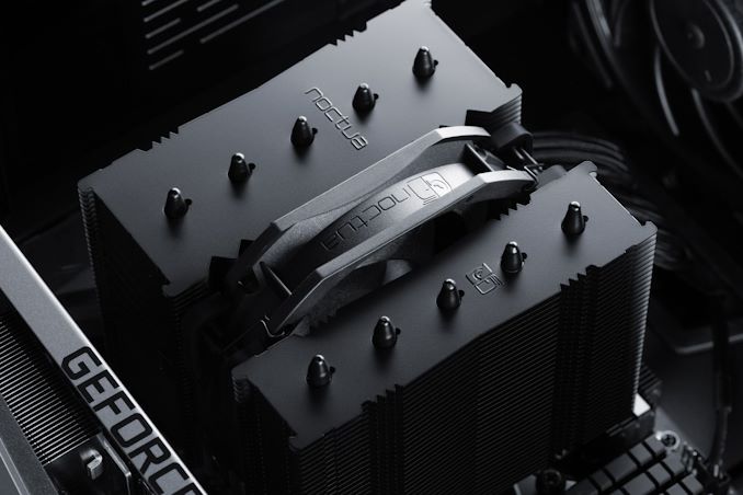
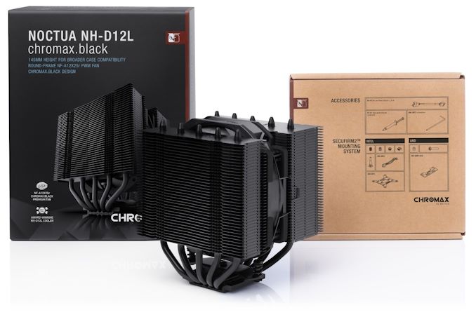
Today, Noctua announced the launch of its NH-D12L chromax.black CPU cooler, an all-black version of the existing NH-D12L. The cooler sports not only a coat of mattte black paint, but also a relatively short height of 145mm, which Noctua says makes the NH-D12L suitable for slimmer cases and 4U server racks.
Having launched in 2022, the NH-D12L is essentially a shorter version of the NH-U12A, which stands at 158mm tall. While plenty of cases have the room for a cooler that tall, not all do (especially small form factor cases). The NH-D12L exists to offer similar performance as the NH-U12A but for cases where 145mm would fit but 158mm wouldn’t. However, the NH-D12L has just a single 120mm NF-A12x25 fan, whereas the NH-U12A has two. Additionally, the NH-D12L has five heatpipes to the NH-U12A’s seven. These two factors mean the NH-D12L can’t quite catch up to the NH-U12A when it comes to cooling capacity.
The chromax.black model is practically identical to the original, but features Noctua’s popular black motif. It should perform the same, and its SecuFirm 2 mounting hardware supports the same sockets: AMD’s AM4 and AM5, and Intel’s LGA 1700 and LGA 1851 for upcoming Arrow Lake CPUs. Despite its compact design, the NH-D12L also has “100% RAM compatibility” for sticks with tall heatspreaders, which sometimes pose clearance issues with air coolers.
The NH-D12L chromax.black also comes with the usual Noctua accessories: a screwdriver, NH-T1 thermal paste, and a four-pin low-noise adapter for the NF-A12x25 fan. Additionally, the 120mm fan is mounted to the cooler via a bracket, meaning no screws are necessary and it can be removed or installed toollessly.
At $99/€109, the NH-D12L is positioned fairly high in the market, next to larger high-end air coolers such as Corsair’s A115, as well as 240mm to 360mm AIO liquid coolers. However, the NH-D12L holds a substantial advantage in its size and compatibility, and while many of these high-end air coolers are 160mm tall or more, the NH-D12L is just 145mm. In some cases, even 15mm could make a big difference.
CPU coolerWestern Digital Ships 24TB Red Pro Hard Drive For NASes [UPDATED] Nowadays highest-capacity hard drives are typically aimed at cloud service providers (CSPs) and enterprises, but this does not mean that creative professionals or regular users do not need them. To cater to demands of more regular consumers, Western Digital has started shipments of its Red Pro 24 TB HDDs, which are aimed at high-end NAS use for creative professionals with significant storage requirements. Western Digital's Red Pro 24 TB hard drives come approximately 20 months after their 22 TB model hit retail in 2022, offering an incremental improvement to WD's highest-capacity NAS and consumer hard drive offering. The platform uses conventional magnetic recording (CMR), feature a 7200 RPM rotating speed, are equipped with a 512 MB cache, and use OptiNAND technology to improve reliability as well as optimize performance and power consumption. The HDDs are rated for an up to 287 MB/s media to cache transfer rate, which makes them some of the fastest hard drives around (albeit, still a bit slower compared to CSP and enterprise-oriented HDDs). Just like other high-end network-attached storage-aimed HDDs, the Red Pro 24 TB hard drives use helium-filled platforms that are very similar to those designed for enterprise drives. Consequently, the Red Pro 24 TB HDD are equipped with rotation vibration sensors to anticipate and proactively counteract disturbances caused by increased vibration and multi-axis shock sensors to detect subtle shock events and automatically offset them with dynamic fly height technology to ensure that heads to not scratch disks. UPDATE 4/2/2024: Western Digital has notified us that WD Red Pro fully support ArmorCache capability, even though it is not listed in datasheets. What these drives lack compared Apparently, just like WD Gold and Ultraster 22 TB and 24 TB drives for enterprises and cloud datacenters, WD Red Pro HDDs fully support the ArmorCache feature that provides protection against power loss when write-cache is enabled (WCE mode) and enhances performance when write-cache is disabled (WCD mode). On the reliability side of matters, Western Digital's Red Pro 24 TB HDDs are designed for 24/7 operation in vibrating environments, such as enterprise-grade NAS with loads of bays, and are rated for up to 550 TB/year workloads as well as up to 600,000 load/unload cycles, which is in line with what Western Digital's WD Gold and Ultrastar hard drives offer. As for power consumption, the WD Red Pro 24 TB consumes up to 6.4W during read and write operations, up to 3.9W in idle mode, and up to 1.2W in standby/sleep mode. Western Digital's Red Pro 24 TB (WD240KFGX) HDDs are now shipping to resellers as well as NAS makers, and are slated to be available shortly. Expect these hard drives to be slightly cheaper than the WD Gold 24 TB model. Storage
NVIDIA's 'cuLitho' Computational Lithography Adopted By TSMC and Synopsys For Production Use Last year, NVIDIA introduced its cuLitho software library, which promises to speed up photomask development by up to 40 times. Today, NVIDIA announced a partnership with TSMC and Synopsys to implement its computational lithography platform for production use, and use the company's next-generation Blackwell GPUs for AI and HPC applications. The development of photomasks is a crucial step for every chip ever made, and NVIDIA's cuLitho platform, enhanced with new generative AI algorithms, significantly speeds up this process. NVIDIA says computational lithography consumes tens of billions of hours per year on CPUs. By leveraging GPU-accelerated computational lithography, cuLitho substantially improves over traditional CPU-based methods. For example, 350 NVIDIA H100 systems can now replace 40,000 CPU systems, resulting in faster production times, lower costs, and reduced space and power requirements. NVIDIA claims its new generative AI algorithms provide an additional 2x speedup on the already accelerated processes enabled through cuLitho. This enhancement is particularly beneficial for the optical proximity correction (OPC) process, allowing the creation of near-perfect inverse masks to account for light diffraction. TSMC says that integrating cuLitho into its workflow has resulted in a 45x speedup of curvilinear flows and an almost 60x improvement in Manhattan-style flows. Curvilinear flows involve mask shapes represented by curves, while Manhattan mask shapes are restricted to horizontal or vertical orientations. Synopsys, a leading developer of electronic design automation (EDA), says that its Proteus mask synthesis software running on the NVIDIA cuLitho software library has accelerated computational workloads compared to current CPU-based methods. This acceleration is crucial for enabling angstrom-level scaling and reducing turnaround time in chip manufacturing. The collaboration between NVIDIA, TSMC, and Synopsys represents a significant advancement in semiconductor manufacturing in general and cuLitho adoption in particular. By leveraging accelerated computing and generative AI, the partners are pushing semiconductor scaling possibilities and opening new innovation opportunities in chip designs. Semiconductors
Under the CHIPS & Science Act, the U.S. government provided tens of billions of dollars in grants and loans to the world's leading maker of chips, such as Intel, Samsung, and TSMC, which will significantly expand the country's semiconductor production industry in the coming years. However, most chips are typically tested, assembled, and packaged in Asia, which has left the American supply chain incomplete. Addressing this last gap in the government's domestic chip production plans, these past couple of weeks the U.S. government signed memorandums of understanding worth about $1.5 billion with Amkor and SK hynix to support their efforts to build chip packaging facilities in the U.S.
Amkor plans to build a $2 billion advanced packaging facility near Peoria, Arizona, to test and assemble chips produced by TSMC at its Fab 21 near Phoenix, Arizona. The company signed a MOU that offers $400 million in direct funding and access to $200 million in loans under the CHIPS & Science Act. In addition, the company plans to take advantage of a 25% investment tax credit on eligible capital expenditures.
Set to be strategically positioned near TSMC's upcoming Fab 21 complex in Arizona, Amkor's Peoria facility will occupy 55 acres and, when fully completed, will feature over 500,000 square feet (46,451 square meters) of cleanroom space, more than twice the size of Amkor's advanced packaging site in Vietnam. Although the company has not disclosed the exact capacity or the specific technologies the facility will support, it is expected to cater to a wide range of industries, including automotive, high-performance computing, and mobile technologies. This suggests the new plant will offer diverse packaging solutions, including traditional, 2.5D, and 3D technologies.
Amkor has collaborated extensively with Apple on the vision and initial setup of the Peoria facility, as Apple is slated to be the facility's first and largest customer, marking a significant commitment from the tech giant. This partnership highlights the importance of the new facility in reinforcing the U.S. semiconductor supply chain and positioning Amkor as a key partner for companies relying on TSMC's manufacturing capabilities. The project is expected to generate around 2,000 jobs and is scheduled to begin operations in 2027.
This week SK hynix also signed a preliminary agreement with the U.S. government to receive up to $450 million in direct funding and $500 million in loans to build an advanced memory packaging facility in West Lafayette, Indiana.
The proposed facility is scheduled to begin operations in 2028, which means that it will assemble HBM4 or HBM4E memory. Meanwhile, DRAM devices for high bandwidth memory (HBM) stacks will still be produced in South Korea. Nonetheless, packing finished HBM4/HBM4E in the U.S. and possibly integrating these memory modules with high-end processors is a big deal.
In addition to building its packaging plant, SK hynix plans to collaborate with Purdue University and other local research institutions to advance semiconductor technology and packaging innovations. This partnership is intended to bolster research and development in the region, positioning the facility as a hub for AI technology and skilled employment.
SemiconductorsStandard CPU coolers, while adequate for managing basic thermal loads, often fall short in terms of noise reduction and superior cooling efficiency. This limitation drives advanced users and system builders to seek aftermarket solutions tailored to their specific needs. The high-end aftermarket cooler market is highly competitive, with manufacturers striving to offer products with exceptional performance.
Endorfy, previously known as SilentiumPC, is a Polish manufacturer that has undergone a significant transformation to expand its presence in global markets. The brand is known for delivering high-performance cooling solutions with a strong focus on balancing efficiency and affordability. By rebranding as Endorfy, the company aims to enter premium market segments while continuing to offer reliable, high-quality cooling products.
SilentiumPC became very popular in the value/mainstream segments of the PC market with their products, the spearhead of which probably was the Fera 5 cooler that we reviewed a little over two years ago and had a remarkable value for money. Today’s review places Endorfy’s largest CPU cooler, the Fortis 5 Dual Fan, on our laboratory test bench. The Fortis 5 is the largest CPU air cooler the company currently offers and is significantly more expensive than the Fera 5, yet it still is a single-tower cooler that strives to strike a balance between value, compatibility, and performance.
Cases/Cooling/PSUsUnder the CHIPS & Science Act, the U.S. government provided tens of billions of dollars in grants and loans to the world's leading maker of chips, such as Intel, Samsung, and TSMC, which will significantly expand the country's semiconductor production industry in the coming years. However, most chips are typically tested, assembled, and packaged in Asia, which has left the American supply chain incomplete. Addressing this last gap in the government's domestic chip production plans, these past couple of weeks the U.S. government signed memorandums of understanding worth about $1.5 billion with Amkor and SK hynix to support their efforts to build chip packaging facilities in the U.S.
Amkor plans to build a $2 billion advanced packaging facility near Peoria, Arizona, to test and assemble chips produced by TSMC at its Fab 21 near Phoenix, Arizona. The company signed a MOU that offers $400 million in direct funding and access to $200 million in loans under the CHIPS & Science Act. In addition, the company plans to take advantage of a 25% investment tax credit on eligible capital expenditures.
Set to be strategically positioned near TSMC's upcoming Fab 21 complex in Arizona, Amkor's Peoria facility will occupy 55 acres and, when fully completed, will feature over 500,000 square feet (46,451 square meters) of cleanroom space, more than twice the size of Amkor's advanced packaging site in Vietnam. Although the company has not disclosed the exact capacity or the specific technologies the facility will support, it is expected to cater to a wide range of industries, including automotive, high-performance computing, and mobile technologies. This suggests the new plant will offer diverse packaging solutions, including traditional, 2.5D, and 3D technologies.
Amkor has collaborated extensively with Apple on the vision and initial setup of the Peoria facility, as Apple is slated to be the facility's first and largest customer, marking a significant commitment from the tech giant. This partnership highlights the importance of the new facility in reinforcing the U.S. semiconductor supply chain and positioning Amkor as a key partner for companies relying on TSMC's manufacturing capabilities. The project is expected to generate around 2,000 jobs and is scheduled to begin operations in 2027.
This week SK hynix also signed a preliminary agreement with the U.S. government to receive up to $450 million in direct funding and $500 million in loans to build an advanced memory packaging facility in West Lafayette, Indiana.
The proposed facility is scheduled to begin operations in 2028, which means that it will assemble HBM4 or HBM4E memory. Meanwhile, DRAM devices for high bandwidth memory (HBM) stacks will still be produced in South Korea. Nonetheless, packing finished HBM4/HBM4E in the U.S. and possibly integrating these memory modules with high-end processors is a big deal.
In addition to building its packaging plant, SK hynix plans to collaborate with Purdue University and other local research institutions to advance semiconductor technology and packaging innovations. This partnership is intended to bolster research and development in the region, positioning the facility as a hub for AI technology and skilled employment.
SemiconductorsIntel has divested its entire stake in Arm Holdings during the second quarter, raising approximately $147 million. Alongside this, Intel sold its stake in cybersecurity firm ZeroFox and reduced its holdings in Astera Labs, all as part of a broader effort to manage costs and recover cash amid significant financial challenges.
The sale of Intel's 1.18 million shares in Arm Holdings, as reported in a recent SEC filing, comes at a time when the company is struggling with substantial financial losses. Despite the $147 million generated from the sale, Intel reported a $120 million net loss on its equity investments for the quarter, which is a part of a larger $1.6 billion loss that Intel faced during this period.
In addition to selling its stake in Arm, Intel also exited its investment in ZeroFox and reduced its involvement with Astera Labs, a company known for developing connectivity platforms for enterprise hardware. These moves are in line with Intel's strategy to reduce costs and stabilize its financial position as it faces ongoing market challenges.
Despite the divestment, Intel's past investment in Arm was likely driven by strategic considerations. Arm Holdings is a significant force in the semiconductor industry, with its designs powering most mobile devices, and, for obvious reasons, Intel would like to address these. Intel and Arm are also collaborating on datacenter platforms tailored for Intel's 18A process technology. Additionally, Arm might view Intel as a potential licensee for its technologies and a valuable partner for other companies that license Arm's designs.
Intel's investment in Astera Labs was also a strategic one as the company probably wanted to secure steady supply of smart retimers, smart cable modems, and CXL memory controller, which are used in volumes in datacenters and Intel is certainly interested in selling as many datacenter CPUs as possible.
Intel's financial struggles were highlighted earlier this month when the company released a disappointing earnings report, which led to a 33% drop in its stock value, erasing billions of dollars of capitalization. To counter these difficulties, Intel announced plans to cut 15,000 jobs and implement other expense reductions. The company has also suspended its dividend, signaling the depth of its efforts to conserve cash and focus on recovery. When it comes to divestment of Arm stock, the need for immediate financial stabilization has presumably taken precedence, leading to the decision.
CPUsUnder the CHIPS & Science Act, the U.S. government provided tens of billions of dollars in grants and loans to the world's leading maker of chips, such as Intel, Samsung, and TSMC, which will significantly expand the country's semiconductor production industry in the coming years. However, most chips are typically tested, assembled, and packaged in Asia, which has left the American supply chain incomplete. Addressing this last gap in the government's domestic chip production plans, these past couple of weeks the U.S. government signed memorandums of understanding worth about $1.5 billion with Amkor and SK hynix to support their efforts to build chip packaging facilities in the U.S.
Amkor plans to build a $2 billion advanced packaging facility near Peoria, Arizona, to test and assemble chips produced by TSMC at its Fab 21 near Phoenix, Arizona. The company signed a MOU that offers $400 million in direct funding and access to $200 million in loans under the CHIPS & Science Act. In addition, the company plans to take advantage of a 25% investment tax credit on eligible capital expenditures.
Set to be strategically positioned near TSMC's upcoming Fab 21 complex in Arizona, Amkor's Peoria facility will occupy 55 acres and, when fully completed, will feature over 500,000 square feet (46,451 square meters) of cleanroom space, more than twice the size of Amkor's advanced packaging site in Vietnam. Although the company has not disclosed the exact capacity or the specific technologies the facility will support, it is expected to cater to a wide range of industries, including automotive, high-performance computing, and mobile technologies. This suggests the new plant will offer diverse packaging solutions, including traditional, 2.5D, and 3D technologies.
Amkor has collaborated extensively with Apple on the vision and initial setup of the Peoria facility, as Apple is slated to be the facility's first and largest customer, marking a significant commitment from the tech giant. This partnership highlights the importance of the new facility in reinforcing the U.S. semiconductor supply chain and positioning Amkor as a key partner for companies relying on TSMC's manufacturing capabilities. The project is expected to generate around 2,000 jobs and is scheduled to begin operations in 2027.
This week SK hynix also signed a preliminary agreement with the U.S. government to receive up to $450 million in direct funding and $500 million in loans to build an advanced memory packaging facility in West Lafayette, Indiana.
The proposed facility is scheduled to begin operations in 2028, which means that it will assemble HBM4 or HBM4E memory. Meanwhile, DRAM devices for high bandwidth memory (HBM) stacks will still be produced in South Korea. Nonetheless, packing finished HBM4/HBM4E in the U.S. and possibly integrating these memory modules with high-end processors is a big deal.
In addition to building its packaging plant, SK hynix plans to collaborate with Purdue University and other local research institutions to advance semiconductor technology and packaging innovations. This partnership is intended to bolster research and development in the region, positioning the facility as a hub for AI technology and skilled employment.
SemiconductorsStandard CPU coolers, while adequate for managing basic thermal loads, often fall short in terms of noise reduction and superior cooling efficiency. This limitation drives advanced users and system builders to seek aftermarket solutions tailored to their specific needs. The high-end aftermarket cooler market is highly competitive, with manufacturers striving to offer products with exceptional performance.
Endorfy, previously known as SilentiumPC, is a Polish manufacturer that has undergone a significant transformation to expand its presence in global markets. The brand is known for delivering high-performance cooling solutions with a strong focus on balancing efficiency and affordability. By rebranding as Endorfy, the company aims to enter premium market segments while continuing to offer reliable, high-quality cooling products.
SilentiumPC became very popular in the value/mainstream segments of the PC market with their products, the spearhead of which probably was the Fera 5 cooler that we reviewed a little over two years ago and had a remarkable value for money. Today’s review places Endorfy’s largest CPU cooler, the Fortis 5 Dual Fan, on our laboratory test bench. The Fortis 5 is the largest CPU air cooler the company currently offers and is significantly more expensive than the Fera 5, yet it still is a single-tower cooler that strives to strike a balance between value, compatibility, and performance.
Cases/Cooling/PSUsUnder the CHIPS & Science Act, the U.S. government provided tens of billions of dollars in grants and loans to the world's leading maker of chips, such as Intel, Samsung, and TSMC, which will significantly expand the country's semiconductor production industry in the coming years. However, most chips are typically tested, assembled, and packaged in Asia, which has left the American supply chain incomplete. Addressing this last gap in the government's domestic chip production plans, these past couple of weeks the U.S. government signed memorandums of understanding worth about $1.5 billion with Amkor and SK hynix to support their efforts to build chip packaging facilities in the U.S.
Amkor plans to build a $2 billion advanced packaging facility near Peoria, Arizona, to test and assemble chips produced by TSMC at its Fab 21 near Phoenix, Arizona. The company signed a MOU that offers $400 million in direct funding and access to $200 million in loans under the CHIPS & Science Act. In addition, the company plans to take advantage of a 25% investment tax credit on eligible capital expenditures.
Set to be strategically positioned near TSMC's upcoming Fab 21 complex in Arizona, Amkor's Peoria facility will occupy 55 acres and, when fully completed, will feature over 500,000 square feet (46,451 square meters) of cleanroom space, more than twice the size of Amkor's advanced packaging site in Vietnam. Although the company has not disclosed the exact capacity or the specific technologies the facility will support, it is expected to cater to a wide range of industries, including automotive, high-performance computing, and mobile technologies. This suggests the new plant will offer diverse packaging solutions, including traditional, 2.5D, and 3D technologies.
Amkor has collaborated extensively with Apple on the vision and initial setup of the Peoria facility, as Apple is slated to be the facility's first and largest customer, marking a significant commitment from the tech giant. This partnership highlights the importance of the new facility in reinforcing the U.S. semiconductor supply chain and positioning Amkor as a key partner for companies relying on TSMC's manufacturing capabilities. The project is expected to generate around 2,000 jobs and is scheduled to begin operations in 2027.
This week SK hynix also signed a preliminary agreement with the U.S. government to receive up to $450 million in direct funding and $500 million in loans to build an advanced memory packaging facility in West Lafayette, Indiana.
The proposed facility is scheduled to begin operations in 2028, which means that it will assemble HBM4 or HBM4E memory. Meanwhile, DRAM devices for high bandwidth memory (HBM) stacks will still be produced in South Korea. Nonetheless, packing finished HBM4/HBM4E in the U.S. and possibly integrating these memory modules with high-end processors is a big deal.
In addition to building its packaging plant, SK hynix plans to collaborate with Purdue University and other local research institutions to advance semiconductor technology and packaging innovations. This partnership is intended to bolster research and development in the region, positioning the facility as a hub for AI technology and skilled employment.
SemiconductorsIntel has divested its entire stake in Arm Holdings during the second quarter, raising approximately $147 million. Alongside this, Intel sold its stake in cybersecurity firm ZeroFox and reduced its holdings in Astera Labs, all as part of a broader effort to manage costs and recover cash amid significant financial challenges.
The sale of Intel's 1.18 million shares in Arm Holdings, as reported in a recent SEC filing, comes at a time when the company is struggling with substantial financial losses. Despite the $147 million generated from the sale, Intel reported a $120 million net loss on its equity investments for the quarter, which is a part of a larger $1.6 billion loss that Intel faced during this period.
In addition to selling its stake in Arm, Intel also exited its investment in ZeroFox and reduced its involvement with Astera Labs, a company known for developing connectivity platforms for enterprise hardware. These moves are in line with Intel's strategy to reduce costs and stabilize its financial position as it faces ongoing market challenges.
Despite the divestment, Intel's past investment in Arm was likely driven by strategic considerations. Arm Holdings is a significant force in the semiconductor industry, with its designs powering most mobile devices, and, for obvious reasons, Intel would like to address these. Intel and Arm are also collaborating on datacenter platforms tailored for Intel's 18A process technology. Additionally, Arm might view Intel as a potential licensee for its technologies and a valuable partner for other companies that license Arm's designs.
Intel's investment in Astera Labs was also a strategic one as the company probably wanted to secure steady supply of smart retimers, smart cable modems, and CXL memory controller, which are used in volumes in datacenters and Intel is certainly interested in selling as many datacenter CPUs as possible.
Intel's financial struggles were highlighted earlier this month when the company released a disappointing earnings report, which led to a 33% drop in its stock value, erasing billions of dollars of capitalization. To counter these difficulties, Intel announced plans to cut 15,000 jobs and implement other expense reductions. The company has also suspended its dividend, signaling the depth of its efforts to conserve cash and focus on recovery. When it comes to divestment of Arm stock, the need for immediate financial stabilization has presumably taken precedence, leading to the decision.
CPUsSamsung had quietly launched its BM1743 enterprise QLC SSD last month with a hefty 61.44 TB SKU. At FMS 2024, the company had the even larger 122.88 TB version of that SSD on display, alongside a few recorded benchmarking sessions. Compared to the previous generation, the BM1743 comes with a 4.1x improvement in I/O performance, improvement in data retention, and a 45% improvement in power efficiency for sequential writes.
The 128 TB-class QLC SSD boasts of sequential read speeds of 7.5 GBps and write speeds of 3 GBps. Random reads come in at 1.6 M IOPS, while 16 KB random writes clock in at 45K IOPS. Based on the quoted random write access granularity, it appears that Samsung is using a 16 KB indirection unit (IU) to optimize flash management. This is similar to the strategy adopted by Solidigm with IUs larger than 4K in their high-capacity SSDs.
A recorded benchmark session on the company's PM9D3a 8-channel Gen 5 SSD was also on display.
The SSD family is being promoted as a mainstream option for datacenters, and boasts of sequential reads up to 12 GBps and writes up to 6.8 GBps. Random reads clock in at 2 M IOPS, and random writes at 400 K IOPS.
Available in multiple form-factors up to 32 TB (M.2 tops out at 2 TB), the drive's firmware includes optional support for flexible data placement (FDP) to help address the write amplification aspect.
The PM1753 is the current enterprise SSD flagship in Samsung's lineup. With support for 16 NAND channels and capacities up to 32 TB, this U.2 / E3.S SSD has advertised sequential read and write speeds of 14.8 GBps and 11 GBps respectively. Random reads and writes for 4 KB accesses are listed at 3.4 M and 600 K IOPS.
Samsung claims a 1.7x performance improvement and a 1.7x power efficiency improvement over the previous generation (PM1743), making this TLC SSD suitable for AI servers.
The 9th Gen. V-NAND wafer was also available for viewing, though photography was prohibited. Mass production of this flash memory began in April 2024.
StorageSamsung had quietly launched its BM1743 enterprise QLC SSD last month with a hefty 61.44 TB SKU. At FMS 2024, the company had the even larger 122.88 TB version of that SSD on display, alongside a few recorded benchmarking sessions. Compared to the previous generation, the BM1743 comes with a 4.1x improvement in I/O performance, improvement in data retention, and a 45% improvement in power efficiency for sequential writes.
The 128 TB-class QLC SSD boasts of sequential read speeds of 7.5 GBps and write speeds of 3 GBps. Random reads come in at 1.6 M IOPS, while 16 KB random writes clock in at 45K IOPS. Based on the quoted random write access granularity, it appears that Samsung is using a 16 KB indirection unit (IU) to optimize flash management. This is similar to the strategy adopted by Solidigm with IUs larger than 4K in their high-capacity SSDs.
A recorded benchmark session on the company's PM9D3a 8-channel Gen 5 SSD was also on display.
The SSD family is being promoted as a mainstream option for datacenters, and boasts of sequential reads up to 12 GBps and writes up to 6.8 GBps. Random reads clock in at 2 M IOPS, and random writes at 400 K IOPS.
Available in multiple form-factors up to 32 TB (M.2 tops out at 2 TB), the drive's firmware includes optional support for flexible data placement (FDP) to help address the write amplification aspect.
The PM1753 is the current enterprise SSD flagship in Samsung's lineup. With support for 16 NAND channels and capacities up to 32 TB, this U.2 / E3.S SSD has advertised sequential read and write speeds of 14.8 GBps and 11 GBps respectively. Random reads and writes for 4 KB accesses are listed at 3.4 M and 600 K IOPS.
Samsung claims a 1.7x performance improvement and a 1.7x power efficiency improvement over the previous generation (PM1743), making this TLC SSD suitable for AI servers.
The 9th Gen. V-NAND wafer was also available for viewing, though photography was prohibited. Mass production of this flash memory began in April 2024.
StorageKioxia's booth at FMS 2024 was a busy one with multiple technology demonstrations keeping visitors occupied. A walk-through of the BiCS 8 manufacturing process was the first to grab my attention. Kioxia and Western Digital announced the sampling of BiCS 8 in March 2023. We had touched briefly upon its CMOS Bonded Array (CBA) scheme in our coverage of Kioxial's 2Tb QLC NAND device and coverage of Western Digital's 128 TB QLC enterprise SSD proof-of-concept demonstration. At Kioxia's booth, we got more insights.
Traditionally, fabrication of flash chips involved placement of the associate logic circuitry (CMOS process) around the periphery of the flash array. The process then moved on to putting the CMOS under the cell array, but the wafer development process was serialized with the CMOS logic getting fabricated first followed by the cell array on top. However, this has some challenges because the cell array requires a high-temperature processing step to ensure higher reliability that can be detrimental to the health of the CMOS logic. Thanks to recent advancements in wafer bonding techniques, the new CBA process allows the CMOS wafer and cell array wafer to be processed independently in parallel and then pieced together, as shown in the models above.
The BiCS 8 3D NAND incorporates 218 layers, compared to 112 layers in BiCS 5 and 162 layers in BiCS 6. The company decided to skip over BiCS 7 (or, rather, it was probably a short-lived generation meant as an internal test vehicle). The generation retains the four-plane charge trap structure of BiCS 6. In its TLC avatar, it is available as a 1 Tbit device. The QLC version is available in two capacities - 1 Tbit and 2 Tbit.
Kioxia also noted that while the number of layers (218) doesn't compare favorably with the latest layer counts from the competition, its lateral scaling / cell shrinkage has enabled it to be competitive in terms of bit density as well as operating speeds (3200 MT/s). For reference, the latest shipping NAND from Micron - the G9 - has 276 layers with a bit density in TLC mode of 21 Gbit/mm2, and operates at up to 3600 MT/s. However, its 232L NAND operates only up to 2400 MT/s and has a bit density of 14.6 Gbit/mm2.
It must be noted that the CBA hybrid bonding process has advantages over the current processes used by other vendors - including Micron's CMOS under array (CuA) and SK hynix's 4D PUC (periphery-under-chip) developed in the late 2010s. It is expected that other NAND vendors will also move eventually to some variant of the hybrid bonding scheme used by Kioxia.
StorageMicrochip recently announced the availability of their second PCIe Gen 5 enterprise SSD controller - the Flashtec 5016. Like the 4016, this is also a 16-channel controller, but there are some key updates:
Microchip's enterprise SSD controllers provide a high level of flexibility to SSD vendors by providing them with significant horsepower and accelerators. The 5016 includes Cortex-A53 cores for SSD vendors to run custom applications relevant to SSD management. However, compared to the Gen4 controllers, there are two additional cores in the CPU cluster. The DRAM subsystem includes ECC support (both out-of-band and inline, as desired by the SSD vendor).
At FMS 2024, the company demonstrated an application of the neural network engines embedded in the Gen5 controllers. Controllers usually employ a 'read-retry' operation with altered read-out voltages for flash reads that do not complete successfully. Microchip implemented a machine learning approach to determine the read-out voltage based on the health history of the NAND block using the NN engines in the controller. This approach delivers tangible benefits for read latency and power consumption (thanks to a smaller number of errors on the first read).
The 4016 and 5016 come with a single-chip root of trust implementation for hardware security. A secure boot process with dual-signature authentication ensures that the controller firmware is not maliciously altered in the field. The company also brought out the advantages of their controller's implementation of SR-IOV, flexible data placement, and zoned namespaces along with their 'credit engine' scheme for multi-tenant cloud workloads. These aspects were also brought out in other demonstrations.
Microchip's press release included quotes from the usual NAND vendors - Solidigm, Kioxia, and Micron. On the customer front, Longsys has been using Flashtec controllers in their enterprise offerings along with YMTC NAND. It is likely that this collaboration will continue further using the new 5016 controller.
StorageA few years back, the Japanese government's New Energy and Industrial Technology Development Organization (NEDO ) allocated funding for the development of green datacenter technologies. With the aim to obtain up to 40% savings in overall power consumption, several Japanese companies have been developing an optical interface for their enterprise SSDs. And at this year's FMS, Kioxia had their optical interface on display.
For this demonstration, Kioxia took its existing CM7 enterprise SSD and created an optical interface for it. A PCIe card with on-board optics developed by Kyocera is installed in the server slot. An optical interface allows data transfer over long distances (it was 40m in the demo, but Kioxia promises lengths of up to 100m for the cable in the future). This allows the storage to be kept in a separate room with minimal cooling requirements compared to the rack with the CPUs and GPUs. Disaggregation of different server components will become an option as very high throughput interfaces such as PCIe 7.0 (with 128 GT/s rates) become available.
The demonstration of the optical SSD showed a slight loss in IOPS performance, but a significant advantage in the latency metric over the shipping enterprise SSD behind a copper network link. Obviously, there are advantages in wiring requirements and signal integrity maintenance with optical links.
Being a proof-of-concept demonstration, we do see the requirement for an industry-standard approach if this were to gain adoption among different datacenter vendors. The PCI-SIG optical workgroup will need to get its act together soon to create a standards-based approach to this problem.
StorageStandard CPU coolers, while adequate for managing basic thermal loads, often fall short in terms of noise reduction and superior cooling efficiency. This limitation drives advanced users and system builders to seek aftermarket solutions tailored to their specific needs. The high-end aftermarket cooler market is highly competitive, with manufacturers striving to offer products with exceptional performance.
Endorfy, previously known as SilentiumPC, is a Polish manufacturer that has undergone a significant transformation to expand its presence in global markets. The brand is known for delivering high-performance cooling solutions with a strong focus on balancing efficiency and affordability. By rebranding as Endorfy, the company aims to enter premium market segments while continuing to offer reliable, high-quality cooling products.
SilentiumPC became very popular in the value/mainstream segments of the PC market with their products, the spearhead of which probably was the Fera 5 cooler that we reviewed a little over two years ago and had a remarkable value for money. Today’s review places Endorfy’s largest CPU cooler, the Fortis 5 Dual Fan, on our laboratory test bench. The Fortis 5 is the largest CPU air cooler the company currently offers and is significantly more expensive than the Fera 5, yet it still is a single-tower cooler that strives to strike a balance between value, compatibility, and performance.
Cases/Cooling/PSUsUnder the CHIPS & Science Act, the U.S. government provided tens of billions of dollars in grants and loans to the world's leading maker of chips, such as Intel, Samsung, and TSMC, which will significantly expand the country's semiconductor production industry in the coming years. However, most chips are typically tested, assembled, and packaged in Asia, which has left the American supply chain incomplete. Addressing this last gap in the government's domestic chip production plans, these past couple of weeks the U.S. government signed memorandums of understanding worth about $1.5 billion with Amkor and SK hynix to support their efforts to build chip packaging facilities in the U.S.
Amkor plans to build a $2 billion advanced packaging facility near Peoria, Arizona, to test and assemble chips produced by TSMC at its Fab 21 near Phoenix, Arizona. The company signed a MOU that offers $400 million in direct funding and access to $200 million in loans under the CHIPS & Science Act. In addition, the company plans to take advantage of a 25% investment tax credit on eligible capital expenditures.
Set to be strategically positioned near TSMC's upcoming Fab 21 complex in Arizona, Amkor's Peoria facility will occupy 55 acres and, when fully completed, will feature over 500,000 square feet (46,451 square meters) of cleanroom space, more than twice the size of Amkor's advanced packaging site in Vietnam. Although the company has not disclosed the exact capacity or the specific technologies the facility will support, it is expected to cater to a wide range of industries, including automotive, high-performance computing, and mobile technologies. This suggests the new plant will offer diverse packaging solutions, including traditional, 2.5D, and 3D technologies.
Amkor has collaborated extensively with Apple on the vision and initial setup of the Peoria facility, as Apple is slated to be the facility's first and largest customer, marking a significant commitment from the tech giant. This partnership highlights the importance of the new facility in reinforcing the U.S. semiconductor supply chain and positioning Amkor as a key partner for companies relying on TSMC's manufacturing capabilities. The project is expected to generate around 2,000 jobs and is scheduled to begin operations in 2027.
This week SK hynix also signed a preliminary agreement with the U.S. government to receive up to $450 million in direct funding and $500 million in loans to build an advanced memory packaging facility in West Lafayette, Indiana.
The proposed facility is scheduled to begin operations in 2028, which means that it will assemble HBM4 or HBM4E memory. Meanwhile, DRAM devices for high bandwidth memory (HBM) stacks will still be produced in South Korea. Nonetheless, packing finished HBM4/HBM4E in the U.S. and possibly integrating these memory modules with high-end processors is a big deal.
In addition to building its packaging plant, SK hynix plans to collaborate with Purdue University and other local research institutions to advance semiconductor technology and packaging innovations. This partnership is intended to bolster research and development in the region, positioning the facility as a hub for AI technology and skilled employment.
SemiconductorsStandard CPU coolers, while adequate for managing basic thermal loads, often fall short in terms of noise reduction and superior cooling efficiency. This limitation drives advanced users and system builders to seek aftermarket solutions tailored to their specific needs. The high-end aftermarket cooler market is highly competitive, with manufacturers striving to offer products with exceptional performance.
Endorfy, previously known as SilentiumPC, is a Polish manufacturer that has undergone a significant transformation to expand its presence in global markets. The brand is known for delivering high-performance cooling solutions with a strong focus on balancing efficiency and affordability. By rebranding as Endorfy, the company aims to enter premium market segments while continuing to offer reliable, high-quality cooling products.
SilentiumPC became very popular in the value/mainstream segments of the PC market with their products, the spearhead of which probably was the Fera 5 cooler that we reviewed a little over two years ago and had a remarkable value for money. Today’s review places Endorfy’s largest CPU cooler, the Fortis 5 Dual Fan, on our laboratory test bench. The Fortis 5 is the largest CPU air cooler the company currently offers and is significantly more expensive than the Fera 5, yet it still is a single-tower cooler that strives to strike a balance between value, compatibility, and performance.
Cases/Cooling/PSUsUnder the CHIPS & Science Act, the U.S. government provided tens of billions of dollars in grants and loans to the world's leading maker of chips, such as Intel, Samsung, and TSMC, which will significantly expand the country's semiconductor production industry in the coming years. However, most chips are typically tested, assembled, and packaged in Asia, which has left the American supply chain incomplete. Addressing this last gap in the government's domestic chip production plans, these past couple of weeks the U.S. government signed memorandums of understanding worth about $1.5 billion with Amkor and SK hynix to support their efforts to build chip packaging facilities in the U.S.
Amkor plans to build a $2 billion advanced packaging facility near Peoria, Arizona, to test and assemble chips produced by TSMC at its Fab 21 near Phoenix, Arizona. The company signed a MOU that offers $400 million in direct funding and access to $200 million in loans under the CHIPS & Science Act. In addition, the company plans to take advantage of a 25% investment tax credit on eligible capital expenditures.
Set to be strategically positioned near TSMC's upcoming Fab 21 complex in Arizona, Amkor's Peoria facility will occupy 55 acres and, when fully completed, will feature over 500,000 square feet (46,451 square meters) of cleanroom space, more than twice the size of Amkor's advanced packaging site in Vietnam. Although the company has not disclosed the exact capacity or the specific technologies the facility will support, it is expected to cater to a wide range of industries, including automotive, high-performance computing, and mobile technologies. This suggests the new plant will offer diverse packaging solutions, including traditional, 2.5D, and 3D technologies.
Amkor has collaborated extensively with Apple on the vision and initial setup of the Peoria facility, as Apple is slated to be the facility's first and largest customer, marking a significant commitment from the tech giant. This partnership highlights the importance of the new facility in reinforcing the U.S. semiconductor supply chain and positioning Amkor as a key partner for companies relying on TSMC's manufacturing capabilities. The project is expected to generate around 2,000 jobs and is scheduled to begin operations in 2027.
This week SK hynix also signed a preliminary agreement with the U.S. government to receive up to $450 million in direct funding and $500 million in loans to build an advanced memory packaging facility in West Lafayette, Indiana.
The proposed facility is scheduled to begin operations in 2028, which means that it will assemble HBM4 or HBM4E memory. Meanwhile, DRAM devices for high bandwidth memory (HBM) stacks will still be produced in South Korea. Nonetheless, packing finished HBM4/HBM4E in the U.S. and possibly integrating these memory modules with high-end processors is a big deal.
In addition to building its packaging plant, SK hynix plans to collaborate with Purdue University and other local research institutions to advance semiconductor technology and packaging innovations. This partnership is intended to bolster research and development in the region, positioning the facility as a hub for AI technology and skilled employment.
Semiconductors
0 Comments