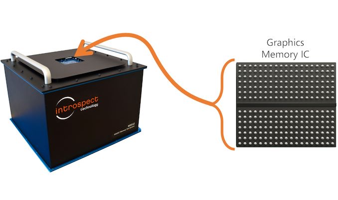
Introspect Intros GDDR7 Test System For Fast GDDR7 GPU Design Bring Up <p align="center"><a href="https://www.anandtech.com/show/21330/introspects-gddr7-test-system-enables-fast-gddr7-gpu-design-bring-up"><img src="https://images.anandtech.com/doci/21330/introspect-gddr7-678b_575px.jpg" alt="" /></a></p><p><p>Introspect this week introduced its M5512 GDDR7 memory test system, which is designed for testing GDDR7 memory controllers, physical interface, and GDDR7 SGRAM chips. The tool will enable memory and processor manufacturers to verify that their products perform as specified by the standard.</p>
<p>One of the crucial phases of a processor design bring up is testing its standard interfaces, such as PCIe, DisplayPort, or GDDR is to ensure that they behave as specified both logically and electrically and achieve designated performance. Introspect's <a href="https://introspect.ca/product/m5512-gddr7-dram-memory-test-system/">M5512 GDDR7 memory test system</a> is designed to do just that: test new GDDR7 memory devices, troubleshoot protocol issues, assess signal integrity, and conduct comprehensive memory read/write stress tests.</p>
<p>The product will be quite useful for designers of GPUs/SoCs, graphics cards, PCs, network equipment and memory chips, which will speed up development of actual products that rely on GDDR7 memory. For now, GPU and SoC designers as well as memory makers use highly-custom setups consisting of many tools to characterize signal integrity as well as conduct detailed memory read/write functional stress testing, which are important things at this phase of development. But usage of a single tool greatly speeds up all the processes and gives a more comprehensive picture to specialists.</p>
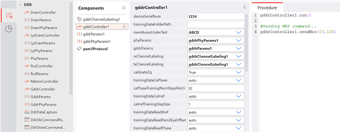
<p style="text-align: center;"><a href="https://www.anandtech.com/show/21330/introspects-gddr7-test-system-enables-fast-gddr7-gpu-design-bring-up"><img alt="" src="https://images.anandtech.com/doci/21330/gd7-gui-screenshot_1200-width_575px.png" /></a></p>
<p>The M5512 GDDR7 Memory Test System is a desktop testing and measurement device that is equippped with 72 pins capable of functioning at up to 40 Gbps in PAM3 mode, as well as offering a virtual GDDR7 memory controller. The device features bidirectional circuitry for executing read and write operations, and every pin is equipped with an extensive range of analog characterization features, such as skew injection with femto-second resolution, voltage control with millivolt resolution, programmable jitter injection, and various eye margining features critical for AC characterization and conformance testing. Furthermore, the system integrates device power supplies with precise power sequencing and ramping controls, providing a comprehensive solution for both AC characterization and memory functional stress testing on any GDDR7 device.</p>
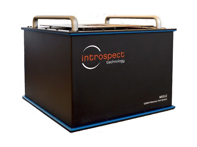
<p align="center"><a href="https://www.anandtech.com/show/21330/introspects-gddr7-test-system-enables-fast-gddr7-gpu-design-bring-up"><img alt="" src="https://images.anandtech.com/doci/21330/M5512-GDDR7-Memory-Test-System-by-Introspect-Technology_575px.jpg" /></a></p>
<p>Introspects M5512 has been designed in close collaboration with JEDEC members working on the GDDR7 specification, so it promises to meet all of their requirements for compliance testing. Notably, however, the device does not eliminate need for interoperability tests and still requires companies to develop their own test algorithms, but it's still a significant tool for bootstrapping device development and getting it to the point where chips can begin interop testing.</p>
<p>“In its quest to support the industry on GDDR7 deployment, Introspect Technology has worked tirelessly in the last few years with JEDEC members to develop the M5512 GDDR7 Memory Test System,” said Dr. Mohamed Hafed, CEO at Introspect Technology.</p>
</p> GPUs
Introspect Intros GDDR7 Test System For Fast GDDR7 GPU Design Bring Up
Introspect this week introduced its M5512 GDDR7 memory test system, which is designed for testing GDDR7 memory controllers, physical interface, and GDDR7 SGRAM chips. The tool will enable memory and processor manufacturers to verify that their products perform as specified by the standard.
One of the crucial phases of a processor design bring up is testing its standard interfaces, such as PCIe, DisplayPort, or GDDR is to ensure that they behave as specified both logically and electrically and achieve designated performance. Introspect's M5512 GDDR7 memory test system is designed to do just that: test new GDDR7 memory devices, troubleshoot protocol issues, assess signal integrity, and conduct comprehensive memory read/write stress tests.
The product will be quite useful for designers of GPUs/SoCs, graphics cards, PCs, network equipment and memory chips, which will speed up development of actual products that rely on GDDR7 memory. For now, GPU and SoC designers as well as memory makers use highly-custom setups consisting of many tools to characterize signal integrity as well as conduct detailed memory read/write functional stress testing, which are important things at this phase of development. But usage of a single tool greatly speeds up all the processes and gives a more comprehensive picture to specialists.
The M5512 GDDR7 Memory Test System is a desktop testing and measurement device that is equippped with 72 pins capable of functioning at up to 40 Gbps in PAM3 mode, as well as offering a virtual GDDR7 memory controller. The device features bidirectional circuitry for executing read and write operations, and every pin is equipped with an extensive range of analog characterization features, such as skew injection with femto-second resolution, voltage control with millivolt resolution, programmable jitter injection, and various eye margining features critical for AC characterization and conformance testing. Furthermore, the system integrates device power supplies with precise power sequencing and ramping controls, providing a comprehensive solution for both AC characterization and memory functional stress testing on any GDDR7 device.
Introspects M5512 has been designed in close collaboration with JEDEC members working on the GDDR7 specification, so it promises to meet all of their requirements for compliance testing. Notably, however, the device does not eliminate need for interoperability tests and still requires companies to develop their own test algorithms, but it's still a significant tool for bootstrapping device development and getting it to the point where chips can begin interop testing.
“In its quest to support the industry on GDDR7 deployment, Introspect Technology has worked tirelessly in the last few years with JEDEC members to develop the M5512 GDDR7 Memory Test System,” said Dr. Mohamed Hafed, CEO at Introspect Technology.


0 Comments