Hot Posts
Intel and Sandia National Labs Roll Out 1.15B Neuron “Hala Point” Neuromorphic Research System
While neuromorphic computing remains under research for the time being, efforts into the field have continued to grow over the years, as have the capabilities of the specialty chips that have been developed for this research. Following those lines, this morning Intel and Sandia National Laboratories are celebrating the deployment of the Hala Point neuromorphic system, which the two believe is the highest capacity system in the world. With 1.15 billion neurons overall, Hala Point is the largest deployment yet for Intel’s Loihi 2 neuromorphic chip, which was first announced at the tail-end of 2021.
The Hala Point system incorporates 1152 Loihi 2 processors, each of which is capable of simulating a million neurons. As noted back at the time of Loihi 2’s launch, these chips are actually rather small – just 31 mm2 per chip with 2.3 billion transistors each, as they’re built on the Intel 4 process (one of the only other Intel chips to do so, besides Meteor Lake). As a result, the complete system is similarly petite, taking up just 6 rack units of space (or as Sandia likes to compare it to, about the size of a microwave), with a power consumption of 2.6 kW. Now that it’s online, Hala Point has dethroned the SpiNNaker system as the largest disclosed neuromorphic system, offering admittedly just a slightly larger number of neurons at less than 3% of the power consumption of the 100 kW British system.
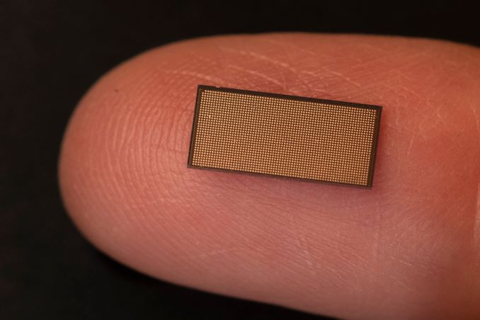
A Single Loihi 2 Chip (31 mm2)
Hala Point will be replacing an older Intel neuromorphic system at Sandia, Pohoiki Springs, which is based on Intel’s first-generation Loihi chips. By comparison, Hala Point offers ten-times as many neurons, and upwards of 12x the performance overall,
Both neuromorphic systems have been procured by Sandia in order to advance the national lab’s research into neuromorphic computing, a computing paradigm that behaves like a brain. The central thought (if you’ll excuse the pun) is that by mimicking the wetware writing this article, neuromorphic chips can be used to solve problems that conventional processors cannot solve today, and that they can do so more efficiently as well.
Sandia, for its part, has said that it will be using the system to look at large-scale neuromorphic computing, with work operating on a scale well beyond Pohoiki Springs. With Hala Point offering a simulated neuron count very roughly on the level of complexity of an owl brain, the lab believes that a larger-scale system will finally enable them to properly exploit the properties of neuromorphic computing to solve real problems in fields such as device physics, computer architecture, computer science and informatics, moving well beyond the simple demonstrations initially achieved at a smaller scale.
One new focus from the lab, which in turn has caught Intel’s attention, is the applicability of neuromorphic computing towards AI inference. Because the neural networks themselves behind the current wave of AI systems are attempting to emulate the human brain, in a sense, there is an obvious degree of synergy with the brain-mimicking neuromorphic chips, even if the algorithms differ in some key respects. Still, with energy efficiency being one of the major benefits of neuromorphic computing, it’s pushed Intel to look into the matter further – and even build a second, Hala Point-sized system of their own.
According to Intel, in their research on Hala Point, the system has reached efficiencies as high as 15 TOPS-per-Watt at 8-bit precision, albeit while using 10:1 sparsity, making it more than competitive with current-generation commercial chips. As an added bonus to that efficiency, the neuromorphic systems don’t require extensive data processing and batching in advance, which is normally necessary to make efficient use of the high density ALU arrays in GPUs and GPU-like processors.
Perhaps the most interesting use case of all, however, is the potent... CPUs
Popular Post
Kioxia Details BiCS 8 NAND at FMS 2024: 218 Layers With Superior Scaling Kioxia's booth at FMS 2024 was a busy one with multiple technology demonstrations keeping visitors occupied. A walk-through of the BiCS 8 manufacturing process was the first to grab my attention. Kioxia and Western Digital announced the sampling of BiCS 8 in March 2023. We had touched briefly upon its CMOS Bonded Array (CBA) scheme in our coverage of Kioxial's 2Tb QLC NAND device and coverage of Western Digital's 128 TB QLC enterprise SSD proof-of-concept demonstration. At Kioxia's booth, we got more insights.
Traditionally, fabrication of flash chips involved placement of the associate logic circuitry (CMOS process) around the periphery of the flash array. The process then moved on to putting the CMOS under the cell array, but the wafer development process was serialized with the CMOS logic getting fabricated first followed by the cell array on top. However, this has some challenges because the cell array requires a high-temperature processing step to ensure higher reliability that can be detrimental to the health of the CMOS logic. Thanks to recent advancements in wafer bonding techniques, the new CBA process allows the CMOS wafer and cell array wafer to be processed independently in parallel and then pieced together, as shown in the models above.
The BiCS 8 3D NAND incorporates 218 layers, compared to 112 layers in BiCS 5 and 162 layers in BiCS 6. The company decided to skip over BiCS 7 (or, rather, it was probably a short-lived generation meant as an internal test vehicle). The generation retains the four-plane charge trap structure of BiCS 6. In its TLC avatar, it is available as a 1 Tbit device. The QLC version is available in two capacities - 1 Tbit and 2 Tbit.
Kioxia also noted that while the number of layers (218) doesn't compare favorably with the latest layer counts from the competition, its lateral scaling / cell shrinkage has enabled it to be competitive in terms of bit density as well as operating speeds (3200 MT/s). For reference, the latest shipping NAND from Micron - the G9 - has 276 layers with a bit density in TLC mode of 21 Gbit/mm2, and operates at up to 3600 MT/s. However, its 232L NAND operates only up to 2400 MT/s and has a bit density of 14.6 Gbit/mm2.
It must be noted that the CBA hybrid bonding process has advantages over the current processes used by other vendors - including Micron's CMOS under array (CuA) and SK hynix's 4D PUC (periphery-under-chip) developed in the late 2010s. It is expected that other NAND vendors will also move eventually to some variant of the hybrid bonding scheme used by Kioxia.
Storage
Kioxia Demonstrates Optical Interface SSDs for Data Centers A few years back, the Japanese government's New Energy and Industrial Technology Development Organization (NEDO ) allocated funding for the development of green datacenter technologies. With the aim to obtain up to 40% savings in overall power consumption, several Japanese companies have been developing an optical interface for their enterprise SSDs. And at this year's FMS, Kioxia had their optical interface on display.
For this demonstration, Kioxia took its existing CM7 enterprise SSD and created an optical interface for it. A PCIe card with on-board optics developed by Kyocera is installed in the server slot. An optical interface allows data transfer over long distances (it was 40m in the demo, but Kioxia promises lengths of up to 100m for the cable in the future). This allows the storage to be kept in a separate room with minimal cooling requirements compared to the rack with the CPUs and GPUs. Disaggregation of different server components will become an option as very high throughput interfaces such as PCIe 7.0 (with 128 GT/s rates) become available.
The demonstration of the optical SSD showed a slight loss in IOPS performance, but a significant advantage in the latency metric over the shipping enterprise SSD behind a copper network link. Obviously, there are advantages in wiring requirements and signal integrity maintenance with optical links.
Being a proof-of-concept demonstration, we do see the requirement for an industry-standard approach if this were to gain adoption among different datacenter vendors. The PCI-SIG optical workgroup will need to get its act together soon to create a standards-based approach to this problem.
Storage
U.S. Signs $1.5B in CHIPS Act Agreements With Amkor and SKhynix for Chip Packaging Plants Under the CHIPS & Science Act, the U.S. government provided tens of billions of dollars in grants and loans to the world's leading maker of chips, such as Intel, Samsung, and TSMC, which will significantly expand the country's semiconductor production industry in the coming years. However, most chips are typically tested, assembled, and packaged in Asia, which has left the American supply chain incomplete. Addressing this last gap in the government's domestic chip production plans, these past couple of weeks the U.S. government signed memorandums of understanding worth about $1.5 billion with Amkor and SK hynix to support their efforts to build chip packaging facilities in the U.S.
Amkor to Build Advanced Packaging Facility with Apple in Mind
Amkor plans to build a $2 billion advanced packaging facility near Peoria, Arizona, to test and assemble chips produced by TSMC at its Fab 21 near Phoenix, Arizona. The company signed a MOU that offers $400 million in direct funding and access to $200 million in loans under the CHIPS & Science Act. In addition, the company plans to take advantage of a 25% investment tax credit on eligible capital expenditures.
Set to be strategically positioned near TSMC's upcoming Fab 21 complex in Arizona, Amkor's Peoria facility will occupy 55 acres and, when fully completed, will feature over 500,000 square feet (46,451 square meters) of cleanroom space, more than twice the size of Amkor's advanced packaging site in Vietnam. Although the company has not disclosed the exact capacity or the specific technologies the facility will support, it is expected to cater to a wide range of industries, including automotive, high-performance computing, and mobile technologies. This suggests the new plant will offer diverse packaging solutions, including traditional, 2.5D, and 3D technologies.
Amkor has collaborated extensively with Apple on the vision and initial setup of the Peoria facility, as Apple is slated to be the facility's first and largest customer, marking a significant commitment from the tech giant. This partnership highlights the importance of the new facility in reinforcing the U.S. semiconductor supply chain and positioning Amkor as a key partner for companies relying on TSMC's manufacturing capabilities. The project is expected to generate around 2,000 jobs and is scheduled to begin operations in 2027.
SK hynix to Build HBM4 in the U.S.
This week SK hynix also signed a preliminary agreement with the U.S. government to receive up to $450 million in direct funding and $500 million in loans to build an advanced memory packaging facility in West Lafayette, Indiana.
The proposed facility is scheduled to begin operations in 2028, which means that it will assemble HBM4 or HBM4E memory. Meanwhile, DRAM devices for high bandwidth memory (HBM) stacks will still be produced in South Korea. Nonetheless, packing finished HBM4/HBM4E in the U.S. and possibly integrating these memory modules with high-end processors is a big deal.
In addition to building its packaging plant, SK hynix plans to collaborate with Purdue University and other local research institutions to advance semiconductor technology and packaging innovations. This partnership is intended to bolster research and development in the region, positioning the facility as a hub for AI technology and skilled employment.
Semiconductors
Kioxia Details BiCS 8 NAND at FMS 2024: 218 Layers With Superior Scaling Kioxia's booth at FMS 2024 was a busy one with multiple technology demonstrations keeping visitors occupied. A walk-through of the BiCS 8 manufacturing process was the first to grab my attention. Kioxia and Western Digital announced the sampling of BiCS 8 in March 2023. We had touched briefly upon its CMOS Bonded Array (CBA) scheme in our coverage of Kioxial's 2Tb QLC NAND device and coverage of Western Digital's 128 TB QLC enterprise SSD proof-of-concept demonstration. At Kioxia's booth, we got more insights.
Traditionally, fabrication of flash chips involved placement of the associate logic circuitry (CMOS process) around the periphery of the flash array. The process then moved on to putting the CMOS under the cell array, but the wafer development process was serialized with the CMOS logic getting fabricated first followed by the cell array on top. However, this has some challenges because the cell array requires a high-temperature processing step to ensure higher reliability that can be detrimental to the health of the CMOS logic. Thanks to recent advancements in wafer bonding techniques, the new CBA process allows the CMOS wafer and cell array wafer to be processed independently in parallel and then pieced together, as shown in the models above.
The BiCS 8 3D NAND incorporates 218 layers, compared to 112 layers in BiCS 5 and 162 layers in BiCS 6. The company decided to skip over BiCS 7 (or, rather, it was probably a short-lived generation meant as an internal test vehicle). The generation retains the four-plane charge trap structure of BiCS 6. In its TLC avatar, it is available as a 1 Tbit device. The QLC version is available in two capacities - 1 Tbit and 2 Tbit.
Kioxia also noted that while the number of layers (218) doesn't compare favorably with the latest layer counts from the competition, its lateral scaling / cell shrinkage has enabled it to be competitive in terms of bit density as well as operating speeds (3200 MT/s). For reference, the latest shipping NAND from Micron - the G9 - has 276 layers with a bit density in TLC mode of 21 Gbit/mm2, and operates at up to 3600 MT/s. However, its 232L NAND operates only up to 2400 MT/s and has a bit density of 14.6 Gbit/mm2.
It must be noted that the CBA hybrid bonding process has advantages over the current processes used by other vendors - including Micron's CMOS under array (CuA) and SK hynix's 4D PUC (periphery-under-chip) developed in the late 2010s. It is expected that other NAND vendors will also move eventually to some variant of the hybrid bonding scheme used by Kioxia.
Storage
Search This Blog
OfferNest
Subscribe Us
Most Popular
Kioxia Details BiCS 8 NAND at FMS 2024: 218 Layers With Superior Scaling Kioxia's booth at FMS 2024 was a busy one with multiple technology demonstrations keeping visitors occupied. A walk-through of the BiCS 8 manufacturing process was the first to grab my attention. Kioxia and Western Digital announced the sampling of BiCS 8 in March 2023. We had touched briefly upon its CMOS Bonded Array (CBA) scheme in our coverage of Kioxial's 2Tb QLC NAND device and coverage of Western Digital's 128 TB QLC enterprise SSD proof-of-concept demonstration. At Kioxia's booth, we got more insights.
Traditionally, fabrication of flash chips involved placement of the associate logic circuitry (CMOS process) around the periphery of the flash array. The process then moved on to putting the CMOS under the cell array, but the wafer development process was serialized with the CMOS logic getting fabricated first followed by the cell array on top. However, this has some challenges because the cell array requires a high-temperature processing step to ensure higher reliability that can be detrimental to the health of the CMOS logic. Thanks to recent advancements in wafer bonding techniques, the new CBA process allows the CMOS wafer and cell array wafer to be processed independently in parallel and then pieced together, as shown in the models above.
The BiCS 8 3D NAND incorporates 218 layers, compared to 112 layers in BiCS 5 and 162 layers in BiCS 6. The company decided to skip over BiCS 7 (or, rather, it was probably a short-lived generation meant as an internal test vehicle). The generation retains the four-plane charge trap structure of BiCS 6. In its TLC avatar, it is available as a 1 Tbit device. The QLC version is available in two capacities - 1 Tbit and 2 Tbit.
Kioxia also noted that while the number of layers (218) doesn't compare favorably with the latest layer counts from the competition, its lateral scaling / cell shrinkage has enabled it to be competitive in terms of bit density as well as operating speeds (3200 MT/s). For reference, the latest shipping NAND from Micron - the G9 - has 276 layers with a bit density in TLC mode of 21 Gbit/mm2, and operates at up to 3600 MT/s. However, its 232L NAND operates only up to 2400 MT/s and has a bit density of 14.6 Gbit/mm2.
It must be noted that the CBA hybrid bonding process has advantages over the current processes used by other vendors - including Micron's CMOS under array (CuA) and SK hynix's 4D PUC (periphery-under-chip) developed in the late 2010s. It is expected that other NAND vendors will also move eventually to some variant of the hybrid bonding scheme used by Kioxia.
Storage
Kioxia Demonstrates Optical Interface SSDs for Data Centers A few years back, the Japanese government's New Energy and Industrial Technology Development Organization (NEDO ) allocated funding for the development of green datacenter technologies. With the aim to obtain up to 40% savings in overall power consumption, several Japanese companies have been developing an optical interface for their enterprise SSDs. And at this year's FMS, Kioxia had their optical interface on display.
For this demonstration, Kioxia took its existing CM7 enterprise SSD and created an optical interface for it. A PCIe card with on-board optics developed by Kyocera is installed in the server slot. An optical interface allows data transfer over long distances (it was 40m in the demo, but Kioxia promises lengths of up to 100m for the cable in the future). This allows the storage to be kept in a separate room with minimal cooling requirements compared to the rack with the CPUs and GPUs. Disaggregation of different server components will become an option as very high throughput interfaces such as PCIe 7.0 (with 128 GT/s rates) become available.
The demonstration of the optical SSD showed a slight loss in IOPS performance, but a significant advantage in the latency metric over the shipping enterprise SSD behind a copper network link. Obviously, there are advantages in wiring requirements and signal integrity maintenance with optical links.
Being a proof-of-concept demonstration, we do see the requirement for an industry-standard approach if this were to gain adoption among different datacenter vendors. The PCI-SIG optical workgroup will need to get its act together soon to create a standards-based approach to this problem.
Storage
U.S. Signs $1.5B in CHIPS Act Agreements With Amkor and SKhynix for Chip Packaging Plants Under the CHIPS & Science Act, the U.S. government provided tens of billions of dollars in grants and loans to the world's leading maker of chips, such as Intel, Samsung, and TSMC, which will significantly expand the country's semiconductor production industry in the coming years. However, most chips are typically tested, assembled, and packaged in Asia, which has left the American supply chain incomplete. Addressing this last gap in the government's domestic chip production plans, these past couple of weeks the U.S. government signed memorandums of understanding worth about $1.5 billion with Amkor and SK hynix to support their efforts to build chip packaging facilities in the U.S.
Amkor to Build Advanced Packaging Facility with Apple in Mind
Amkor plans to build a $2 billion advanced packaging facility near Peoria, Arizona, to test and assemble chips produced by TSMC at its Fab 21 near Phoenix, Arizona. The company signed a MOU that offers $400 million in direct funding and access to $200 million in loans under the CHIPS & Science Act. In addition, the company plans to take advantage of a 25% investment tax credit on eligible capital expenditures.
Set to be strategically positioned near TSMC's upcoming Fab 21 complex in Arizona, Amkor's Peoria facility will occupy 55 acres and, when fully completed, will feature over 500,000 square feet (46,451 square meters) of cleanroom space, more than twice the size of Amkor's advanced packaging site in Vietnam. Although the company has not disclosed the exact capacity or the specific technologies the facility will support, it is expected to cater to a wide range of industries, including automotive, high-performance computing, and mobile technologies. This suggests the new plant will offer diverse packaging solutions, including traditional, 2.5D, and 3D technologies.
Amkor has collaborated extensively with Apple on the vision and initial setup of the Peoria facility, as Apple is slated to be the facility's first and largest customer, marking a significant commitment from the tech giant. This partnership highlights the importance of the new facility in reinforcing the U.S. semiconductor supply chain and positioning Amkor as a key partner for companies relying on TSMC's manufacturing capabilities. The project is expected to generate around 2,000 jobs and is scheduled to begin operations in 2027.
SK hynix to Build HBM4 in the U.S.
This week SK hynix also signed a preliminary agreement with the U.S. government to receive up to $450 million in direct funding and $500 million in loans to build an advanced memory packaging facility in West Lafayette, Indiana.
The proposed facility is scheduled to begin operations in 2028, which means that it will assemble HBM4 or HBM4E memory. Meanwhile, DRAM devices for high bandwidth memory (HBM) stacks will still be produced in South Korea. Nonetheless, packing finished HBM4/HBM4E in the U.S. and possibly integrating these memory modules with high-end processors is a big deal.
In addition to building its packaging plant, SK hynix plans to collaborate with Purdue University and other local research institutions to advance semiconductor technology and packaging innovations. This partnership is intended to bolster research and development in the region, positioning the facility as a hub for AI technology and skilled employment.
Semiconductors
Kioxia Details BiCS 8 NAND at FMS 2024: 218 Layers With Superior Scaling Kioxia's booth at FMS 2024 was a busy one with multiple technology demonstrations keeping visitors occupied. A walk-through of the BiCS 8 manufacturing process was the first to grab my attention. Kioxia and Western Digital announced the sampling of BiCS 8 in March 2023. We had touched briefly upon its CMOS Bonded Array (CBA) scheme in our coverage of Kioxial's 2Tb QLC NAND device and coverage of Western Digital's 128 TB QLC enterprise SSD proof-of-concept demonstration. At Kioxia's booth, we got more insights.
Traditionally, fabrication of flash chips involved placement of the associate logic circuitry (CMOS process) around the periphery of the flash array. The process then moved on to putting the CMOS under the cell array, but the wafer development process was serialized with the CMOS logic getting fabricated first followed by the cell array on top. However, this has some challenges because the cell array requires a high-temperature processing step to ensure higher reliability that can be detrimental to the health of the CMOS logic. Thanks to recent advancements in wafer bonding techniques, the new CBA process allows the CMOS wafer and cell array wafer to be processed independently in parallel and then pieced together, as shown in the models above.
The BiCS 8 3D NAND incorporates 218 layers, compared to 112 layers in BiCS 5 and 162 layers in BiCS 6. The company decided to skip over BiCS 7 (or, rather, it was probably a short-lived generation meant as an internal test vehicle). The generation retains the four-plane charge trap structure of BiCS 6. In its TLC avatar, it is available as a 1 Tbit device. The QLC version is available in two capacities - 1 Tbit and 2 Tbit.
Kioxia also noted that while the number of layers (218) doesn't compare favorably with the latest layer counts from the competition, its lateral scaling / cell shrinkage has enabled it to be competitive in terms of bit density as well as operating speeds (3200 MT/s). For reference, the latest shipping NAND from Micron - the G9 - has 276 layers with a bit density in TLC mode of 21 Gbit/mm2, and operates at up to 3600 MT/s. However, its 232L NAND operates only up to 2400 MT/s and has a bit density of 14.6 Gbit/mm2.
It must be noted that the CBA hybrid bonding process has advantages over the current processes used by other vendors - including Micron's CMOS under array (CuA) and SK hynix's 4D PUC (periphery-under-chip) developed in the late 2010s. It is expected that other NAND vendors will also move eventually to some variant of the hybrid bonding scheme used by Kioxia.
Storage
Samsung's 128 TB-Class BM1743 Enterprise SSD Displayed at FMS 2024 Samsung had quietly launched its BM1743 enterprise QLC SSD last month with a hefty 61.44 TB SKU. At FMS 2024, the company had the even larger 122.88 TB version of that SSD on display, alongside a few recorded benchmarking sessions. Compared to the previous generation, the BM1743 comes with a 4.1x improvement in I/O performance, improvement in data retention, and a 45% improvement in power efficiency for sequential writes.
The 128 TB-class QLC SSD boasts of sequential read speeds of 7.5 GBps and write speeds of 3 GBps. Random reads come in at 1.6 M IOPS, while 16 KB random writes clock in at 45K IOPS. Based on the quoted random write access granularity, it appears that Samsung is using a 16 KB indirection unit (IU) to optimize flash management. This is similar to the strategy adopted by Solidigm with IUs larger than 4K in their high-capacity SSDs.
A recorded benchmark session on the company's PM9D3a 8-channel Gen 5 SSD was also on display.
The SSD family is being promoted as a mainstream option for datacenters, and boasts of sequential reads up to 12 GBps and writes up to 6.8 GBps. Random reads clock in at 2 M IOPS, and random writes at 400 K IOPS.
Available in multiple form-factors up to 32 TB (M.2 tops out at 2 TB), the drive's firmware includes optional support for flexible data placement (FDP) to help address the write amplification aspect.
The PM1753 is the current enterprise SSD flagship in Samsung's lineup. With support for 16 NAND channels and capacities up to 32 TB, this U.2 / E3.S SSD has advertised sequential read and write speeds of 14.8 GBps and 11 GBps respectively. Random reads and writes for 4 KB accesses are listed at 3.4 M and 600 K IOPS.
Samsung claims a 1.7x performance improvement and a 1.7x power efficiency improvement over the previous generation (PM1743), making this TLC SSD suitable for AI servers.
The 9th Gen. V-NAND wafer was also available for viewing, though photography was prohibited. Mass production of this flash memory began in April 2024.
Storage
Western Digital Introduces 4 TB microSDUC, 8 TB SDUC, and 16 TB External SSDs Western Digital's BiCS8 218-layer 3D NAND is being put to good use in a wide range of client and enterprise platforms, including WD's upcoming Gen 5 client SSDs and 128 TB-class datacenter SSD. On the external storage front, the company demonstrated four different products: for card-based media, 4 TB microSDUC and 8 TB SDUC cards with UHS-I speeds, and on the portable SSD front we had two 16 TB drives. One will be a SanDisk Desk Drive with external power, and the other in the SanDisk Extreme Pro housing with a lanyard opening in the case.
All of these are using BiCS8 QLC NAND, though I did hear booth talk (as I was taking leave) that they were not supposed to divulge the use of QLC in these products. The 4 TB microSDUC and 8 TB SDUC cards are rated for UHS-I speeds. They are being marketed under the SanDisk Ultra branding.
The SanDisk Desk Drive is an external SSD with a 18W power adapter, and it has been in the market for a few months now. Initially launched in capacities up to 8 TB, Western Digital had promised a 16 TB version before the end of the year. It appears that the product is coming to retail quite soon. One aspect to note is that this drive has been using TLC for the SKUs that are currently in the market, so it appears unlikely that the 16 TB version would be QLC. The units (at least up to the 8 TB capacity point) come with two SN850XE drives. Given the recent introduction of the 8 TB SN850X, an 'E' version with tweaked firmware is likely to be present in the 16 TB Desk Drive.
The 16 TB portable SSD in the SanDisk Extreme housing was a technology demonstration. It is definitely the highest capacity bus-powered portable SSD demonstrated by any vendor at any trade show thus far. Given the 16 TB Desk Drive's imminent market introduction, it is just a matter of time before the technology demonstration of the bus-powered version becomes a retail reality.
Storage
End of the Road: An AnandTech Farewell It is with great sadness that I find myself penning the hardest news post I’ve ever needed to write here at AnandTech. After over 27 years of covering the wide – and wild – world of computing hardware, today is AnandTech’s final day of publication.
For better or worse, we’ve reached the end of a long journey – one that started with a review of an AMD processor, and has ended with the review of an AMD processor. It’s fittingly poetic, but it is also a testament to the fact that we’ve spent the last 27 years doing what we love, covering the chips that are the lifeblood of the computing industry.
A lot of things have changed in the last quarter-century – in 1997 NVIDIA had yet to even coin the term “GPU” – and we’ve been fortunate to watch the world of hardware continue to evolve over the time period. We’ve gone from boxy desktop computers and laptops that today we’d charitably classify as portable desktops, to pocket computers where even the cheapest budget device puts the fastest PC of 1997 to shame.
The years have also brought some monumental changes to the world of publishing. AnandTech was hardly the first hardware enthusiast website, nor will we be the last. But we were fortunate to thrive in the past couple of decades, when so many of our peers did not, thanks to a combination of hard work, strategic investments in people and products, even more hard work, and the support of our many friends, colleagues, and readers.
Still, few things last forever, and the market for written tech journalism is not what it once was – nor will it ever be again. So, the time has come for AnandTech to wrap up its work, and let the next generation of tech journalists take their place within the zeitgeist.
It has been my immense privilege to write for AnandTech for the past 19 years – and to manage it as its editor-in-chief for the past decade. And while I carry more than a bit of remorse in being AnandTech’s final boss, I can at least take pride in everything we’ve accomplished over the years, whether it’s lauding some legendary products, writing technology primers that still remain relevant today, or watching new stars rise in expected places. There is still more that I had wanted AnandTech to do, but after 21,500 articles, this was a good start.
And while the AnandTech staff is riding off into the sunset, I am happy to report that the site itself won’t be going anywhere for a while. Our publisher, Future PLC, will be keeping the AnandTech website and its many articles live indefinitely. So that all of the content we’ve created over the years remains accessible and citable. Even without new articles to add to the collection, I expect that many of the things we’ve written over the past couple of decades will remain relevant for years to come – and remain accessible just as long.
The AnandTech Forums will also continue to be operated by Future’s community team and our dedicated troop of moderators. With forum threads going back to 1999 (and some active members just as long), the forums have a history almost as long and as storied as AnandTech itself (wounded monitor children, anyone?). So even when AnandTech is no longer publishing articles, we’ll still have a place for everyone to talk about the latest in technology – and have those discussions last longer than 48 hours.
Finally, for everyone who still needs their technical writing fix, our formidable opposition of the last 27 years and fellow Future brand, Tom’s Hardware, is continuing to cover the world of technology. There are a couple of familiar AnandTech faces already over there providing their accumulated expertise, and the site will continue doing its best to provide a written take on technology news.
So Many Thank Yous
As I look back on everything AnandTech has accomplished over the past 27 years, there are more than a few people, groups, and companies that I would like to thank on behalf of both myself and AnandTech as a whole.
First and foremost, I cannot thank enough all the editors who have worked for AnandTech over the years. T... Site Updates
Tags
- https://www.amazon.com/2020-2021-Planner-Academic-Do-Twin-Wire/dp/B083V11TM5?tag=all0ad0-21https://m.media-amazon.com/images/I/41btLRSWksL.jpg
- https://www.amazon.com/Acid-Dreams-Complete-History-Sixties-ebook/dp/B005012G6U?tag=all0ad0-21https://m.media-amazon.com/images/I/51SwQkWyzAL.jpg
- https://www.amazon.com/Adaptive-Charging-Charger-Compatible-EP-TA20JBE/dp/B07NPD5T5H?tag=all0ad0-21https://m.media-amazon.com/images/I/419ZKbzdOwL.jpg
- https://www.amazon.com/Adjustable-Foldable-Portable-Compatible-Smartphones/dp/B0963PBY4C?tag=all0ad0-21https://m.media-amazon.com/images/I/51p4wF13kCL.jpg
- https://www.amazon.com/African-Twisted-Headwraps-Headband-Headscarf/dp/B09FDMKTZP?tag=all0ad0-21https://m.media-amazon.com/images/I/41WGbzL+RkL.jpg
- https://www.amazon.com/AINOPE-Charging-Braided-compatible-MacBook/dp/B094YDZQ1C?tag=all0ad0-21https://m.media-amazon.com/images/I/51ppc0xIVtL.jpg
- https://www.amazon.com/Ambergris-Saints-Madmen-Shriek-Finch/dp/B08GGCSN3S?tag=all0ad0-21https://m.media-amazon.com/images/I/51zgVCTiUiL.jpg
- https://www.amazon.com/Amplim-Hospital-Thermometer-Professional-Thermometer/dp/B0865R5H82?tag=all0ad0-21https://m.media-amazon.com/images/I/31K01H4s6UL.jpg
- https://www.amazon.com/Animal-Gaming-Electronic-Lights-Birthday/dp/B0B2QTLWMS?tag=all0ad0-21https://m.media-amazon.com/images/I/41GY22qHwkL.jpg
- https://www.amazon.com/Animals-Flashcards-Children-Alphabet-cards/dp/9811168881?tag=all0ad0-21https://m.media-amazon.com/images/I/51U2gcSb62L.jpg
- https://www.amazon.com/ANNKIE-Dance-Electronic-Lights-Birthday/dp/B0B74DVQQV?tag=all0ad0-21https://m.media-amazon.com/images/I/51K45aP99DL.jpg
- https://www.amazon.com/Anti-Wrinkle-Silicone-Reusable-D%C3%A9collet%C3%A9-Eliminate/dp/B07FQ3QV1C?tag=all0ad0-21https://m.media-amazon.com/images/I/41RhHEsEi3L.jpg
- https://www.amazon.com/anyloop-Military-Smartwatch-Bluetooth-Waterproof/dp/B0C4P7R6CK?tag=all0ad0-21https://m.media-amazon.com/images/I/41lUAHTmi5L.jpg
- https://www.amazon.com/Aromatherapy-Shower-Steamers-Relaxation-Everything/dp/B08QDKWBWS?tag=all0ad0-21https://m.media-amazon.com/images/I/613KwmLJJ1L.jpg
- https://www.amazon.com/Audible-A-Rose-in-Winter/dp/B09JHTGT14?tag=all0ad0-21https://m.media-amazon.com/images/I/51z1bVj4CxL.jpg
- https://www.amazon.com/Audible-Fall-School-Good-Evil/dp/B0B8SZY3P5?tag=all0ad0-21https://m.media-amazon.com/images/I/51MWO0bOLIL.jpg
- https://www.amazon.com/Audible-Termination-Shock-A-Novel/dp/B09556Y79B?tag=all0ad0-21https://m.media-amazon.com/images/I/51jEsfJXG3S.jpg
- https://www.amazon.com/Automatic-Toddlers-Operated-Batteries-Birthday/dp/B0BZH34G2G?tag=all0ad0-21https://m.media-amazon.com/images/I/51PQaTAouaL.jpg
- https://www.amazon.com/AWGOU-Baby-Wipes-Dispenser-Large-Capacity/dp/B0BS3K9BFV?tag=all0ad0-21https://m.media-amazon.com/images/I/41emlsr6WnL.jpg
- https://www.amazon.com/AYAO-Blades-8-Inch-12TPI-2-Pack/dp/B0C9C1VB3D?tag=all0ad0-21https://m.media-amazon.com/images/I/41jMumgfJ4L.jpg
- https://www.amazon.com/Backless-Sleeve-Ribbed-Fitted-Shirts/dp/B0B68KPGP8?tag=all0ad0-21https://m.media-amazon.com/images/I/41vB0uLnuzL.jpg
- https://www.amazon.com/BCHWAY-Stuffed-Storage-Beanbag-Organizer/dp/B09WR2KPPG?tag=all0ad0-21https://m.media-amazon.com/images/I/41GBr+1tEBL.jpg
- https://www.amazon.com/beeprt-Bluetooth-Shipping-Label-Printer/dp/B0BK93ZSNC?tag=all0ad0-21https://m.media-amazon.com/images/I/41Ufm05KrJL.jpg
- https://www.amazon.com/Benewid-Creami-Pints-Lids-Containers/dp/B0C85Q44N6?tag=all0ad0-21https://m.media-amazon.com/images/I/41bFv6o0xjL.jpg
- https://www.amazon.com/BIG-TEETH-Magnetic-Microfiber-5-Piece/dp/B0BRXBM2T9?tag=all0ad0-21https://m.media-amazon.com/images/I/51BCt4B8jDL.jpg
- https://www.amazon.com/Blackbeard-Americas-Most-Notorious-Pirate/dp/B086N4X4SG?tag=all0ad0-21https://m.media-amazon.com/images/I/51fqeuICW+L.jpg
- https://www.amazon.com/Blaster-Automatic-Toddlers-Christmas-Birthday/dp/B0CCV9RDM5?tag=all0ad0-21https://m.media-amazon.com/images/I/51j8FkZtBiL.jpg
- https://www.amazon.com/Bloodline-Jess-Lourey/dp/1542016312?tag=all0ad0-21https://m.media-amazon.com/images/I/51KLqBsOIbL.jpg
- https://www.amazon.com/Bracelet-Stainless-Zirconium-Ceramic-Statement/dp/B0B2CQR5YW?tag=all0ad0-21https://m.media-amazon.com/images/I/41iUmnfsAmL.jpg
- https://www.amazon.com/Bride-Shadow-King-Book/dp/B0B75RL7DX?tag=all0ad0-21https://m.media-amazon.com/images/I/51LyIt-n5+L.jpg
- https://www.amazon.com/Bright-Empires-House-Spirit-Shadow/dp/B08T4VG1S2?tag=all0ad0-21https://m.media-amazon.com/images/I/61-JxjVNClL.jpg
- https://www.amazon.com/BRIGHTWORLD-Stuffers-Upgrade-5-9inch-Birthday/dp/B0B6RBCYZ7?tag=all0ad0-21https://m.media-amazon.com/images/I/61pQaIf3NVL.jpg
- https://www.amazon.com/Bunfly-Clipper-Grooming-Suction-Capacity/dp/B0C6PMSY3Z?tag=all0ad0-21https://m.media-amazon.com/images/I/51ig7m1g9OL.jpg
- https://www.amazon.com/C412H-Spring-Wound-Commercial-12-Hour-Automatic/dp/B00CTW2LYA?tag=all0ad0-21https://m.media-amazon.com/images/I/41QNVA+3MRL.jpg
- https://www.amazon.com/Cardone-Select-84-832-Ignition-Distributor/dp/B000CFFAYY?tag=all0ad0-21https://m.media-amazon.com/images/I/414iGfzryML.jpg
- https://www.amazon.com/ceiba-tree-Graduation-Envelopes-Classroom/dp/B0BQQKSLFK?tag=all0ad0-21https://m.media-amazon.com/images/I/51ZOS4YOvzL.jpg
- https://www.amazon.com/CellElection-Elastic-Ponytail-Holders-Straight/dp/B09TFDLR85?tag=all0ad0-21https://m.media-amazon.com/images/I/514QbooGKKL.jpg
- https://www.amazon.com/Certified-Charger-Charging-Braveridge-Lightning/dp/B0C1VKRXN1?tag=all0ad0-21https://m.media-amazon.com/images/I/41XG+lopk8L.jpg
- https://www.amazon.com/Certified%E3%80%91-Charger-Fasting-Charging-Compatible/dp/B0C489SXGB?tag=all0ad0-21https://m.media-amazon.com/images/I/41dNzZS3BML.jpg
- https://www.amazon.com/Charger-Certified-Lightning-Charging-Compatible/dp/B0C4L9S7QH?tag=all0ad0-21https://m.media-amazon.com/images/I/514iP4Fy28L.jpg
- https://www.amazon.com/Chicken-Shredder-Ergonomic-Anti-Slip-Dishwasher/dp/B0C5R1KZP6?tag=all0ad0-21https://m.media-amazon.com/images/I/61cx6f737WL.jpg
- https://www.amazon.com/Christmas-Decorations-PHITRIC-Sparkling-Fireplace/dp/B0B7WNC93J?tag=all0ad0-21https://m.media-amazon.com/images/I/51Gv07W+JCL.jpg
- https://www.amazon.com/Christmas-Snowflake-Stamping-Manicure-Designer/dp/B09L4SV5YY?tag=all0ad0-21https://m.media-amazon.com/images/I/51TQJxPWLrL.jpg
- https://www.amazon.com/Cleaning-Bathroom-Crevice-Bristle-Multifunctional/dp/B0CDBK4C9T?tag=all0ad0-21https://m.media-amazon.com/images/I/415dsUeaDmL.jpg
- https://www.amazon.com/Clinic-Crohns-Disease-Ulcerative-Colitis-ebook/dp/B09ZBLJLFL?tag=all0ad0-21https://m.media-amazon.com/images/I/41f5FHJle+L.jpg
- https://www.amazon.com/Coasters-Absorbent-Ceramic-Coaster-Housewarming/dp/B09ZKJRSLH?tag=all0ad0-21https://m.media-amazon.com/images/I/51POqbEgyOL.jpg
- https://www.amazon.com/CoBak-Rotating-Case-iPad-Generation/dp/B0BBR8MFHM?tag=all0ad0-21https://m.media-amazon.com/images/I/516NR1N0QKL.jpg
- https://www.amazon.com/COLORFULLEAF-Bamboo-Underwear-Breathable-Trunks/dp/B0B9BX5S9L?tag=all0ad0-21https://m.media-amazon.com/images/I/31MYPhHHapL.jpg
- https://www.amazon.com/Comforter-Paisley-Microfiber-Bohemian-Pillowcases/dp/B0BZP1SC6F?tag=all0ad0-21https://m.media-amazon.com/images/I/51KkoN3AgNL.jpg
- https://www.amazon.com/Compressed-Cordless-Electric-Brushless-Portable/dp/B0BBR1XHLS?tag=all0ad0-21https://m.media-amazon.com/images/I/41dJ2sJpGjL.jpg
- https://www.amazon.com/Cordking-14-Protectors-Shockproof-Microfiber/dp/B0B6GKRCGM?tag=all0ad0-21https://m.media-amazon.com/images/I/41tXMeWi5FL.jpg
- https://www.amazon.com/Cordless-High-Speed-Brushless-Lightweight-Cleaners/dp/B0CGL8NBM8?tag=all0ad0-21https://m.media-amazon.com/images/I/41NfsXSEnLL.jpg
- https://www.amazon.com/Cordless-Straightening-Travel-Wireless-Straightener/dp/B0CJ2HQL3H?tag=all0ad0-21https://m.media-amazon.com/images/I/31wTmdUZyuL.jpg
- https://www.amazon.com/Corrector-Clavicle-Adjustable-Straightener-Providing/dp/B07L41CV8B?tag=all0ad0-21https://m.media-amazon.com/images/I/41B0xbK2kRL.jpg
- https://www.amazon.com/Court-Wizard-Terry-Mancour-audiobook/dp/B07PC2RQSC?tag=all0ad0-21https://m.media-amazon.com/images/I/512jFQbt6JL.jpg
- https://www.amazon.com/Cozivwaiy-Platform-Sandals-Studded-Evening/dp/B0BM43W7VF?tag=all0ad0-21https://m.media-amazon.com/images/I/41+RFM1gP7L.jpg
- https://www.amazon.com/Crenova-Magnetic-Construction-Preschool-Educational/dp/B0CC1RZ2BJ?tag=all0ad0-21https://m.media-amazon.com/images/I/51lJxAlaL3L.jpg
- https://www.amazon.com/Dan-Darci-Marbling-Paint-Kids/dp/B08CLVVJ8C?tag=all0ad0-21https://m.media-amazon.com/images/I/61nDIOC0B0L.jpg
- https://www.amazon.com/Dash-Cam-Front-BOOGIIO-Dashboard/dp/B08LZJ8GMH?tag=all0ad0-21https://m.media-amazon.com/images/I/41B3QK42N1L.jpg
- https://www.amazon.com/Democracy-America-What-Wrong-About-ebook/dp/B0867TRV52?tag=all0ad0-21https://m.media-amazon.com/images/I/4129LSadlmL.jpg
- https://www.amazon.com/Detailing-Attachment-Scrubber-Cleaning-Upholstery/dp/B07WGKQVN7?tag=all0ad0-21https://m.media-amazon.com/images/I/41K75BhGaML.jpg
- https://www.amazon.com/Diameter-Hydrophilic-Filtration-Non-sterile-COBETTER/dp/B0B7BB3L1R?tag=all0ad0-21https://m.media-amazon.com/images/I/31KD4E7TW5L.jpg
- https://www.amazon.com/Diamond-Organizer-Jewelry-Storage-Diamonds/dp/B08JLVSZ15?tag=all0ad0-21https://m.media-amazon.com/images/I/514Z+bbZfQL.jpg
- https://www.amazon.com/Diamond-Painting-Diamonds-12x16inch-30%C3%9740cm/dp/B09X1CQJHX?tag=all0ad0-21https://m.media-amazon.com/images/I/51xEpqCkI-L.jpg
- https://www.amazon.com/didforu-Monocular-Telescope-Monoscope-Binocular/dp/B0C3757D5G?tag=all0ad0-21https://m.media-amazon.com/images/I/512qer0p1oL.jpg
- https://www.amazon.com/Dinkhiiro-Outdoor-Pickleball-Balls-Pickle-Ball-Accessories-Pickleball/dp/B0BNQ8HM76?tag=all0ad0-21https://m.media-amazon.com/images/I/41ni+GPR71L.jpg
- https://www.amazon.com/Distant-Horizon-Backyard-Starship-Book/dp/B0BDP9RPQL?tag=all0ad0-21https://m.media-amazon.com/images/I/512FYS+c9wL.jpg
- https://www.amazon.com/Dorman-1650134-Chevrolet-Driver-Assembly/dp/B00JW1XGDG?tag=all0ad0-21https://m.media-amazon.com/images/I/51p-ja2Vc9L.jpg
- https://www.amazon.com/DosTutu-Mermaid-Costume-Pageant-Birthday/dp/B09NJK6K9M?tag=all0ad0-21https://m.media-amazon.com/images/I/51pVYQBZKJL.jpg
- https://www.amazon.com/dp/B09GFWPXWH?tag=all0ad0-21https://m.media-amazon.com/images/I/51xO7ZL-sVL.jpg
- https://www.amazon.com/DREAMS-VISIONS-Jesus-Awakening-Muslim-ebook/dp/B0078FAA3M?tag=all0ad0-21https://m.media-amazon.com/images/I/51BKVftuXDL.jpg
- https://www.amazon.com/DSJUGGLING-Transparent-Two-Tone-Juggling-Beginners/dp/B09WHRZCFF?tag=all0ad0-21https://m.media-amazon.com/images/I/419NOeSGijL.jpg
- https://www.amazon.com/Empire-of-Storms-Sarah-J-Maas-audiobook/dp/B01KIQV5EU?tag=all0ad0-21https://m.media-amazon.com/images/I/51EMceUgxFL.jpg
- https://www.amazon.com/Eniucow-Montessori-Permanent-Traction-Toddlers/dp/B0B7CZ9KGN?tag=all0ad0-21https://m.media-amazon.com/images/I/31bJyZYqhJL.jpg
- https://www.amazon.com/Eslazoer-insulated-neoprene-reusable-activity/dp/B0BKSMXVN8?tag=all0ad0-21https://m.media-amazon.com/images/I/41kTXH2JxBL.jpg
- https://www.amazon.com/Everyday-Solutions-Mug-Tree-Polished/dp/B0B4T6NCML?tag=all0ad0-21https://m.media-amazon.com/images/I/31-7RTd1fUL.jpg
- https://www.amazon.com/Extender-Universal-Rotatable-Extension-Attachment/dp/B0C4YLVH3D?tag=all0ad0-21https://m.media-amazon.com/images/I/41+YysChcFL.jpg
- https://www.amazon.com/Eyelash-Extension-Cleanser-BREYLEE-Shampoo/dp/B08RJFTFN4?tag=all0ad0-21https://m.media-amazon.com/images/I/51UncwwSzwL.jpg
- https://www.amazon.com/Fatal-Discord-Michael-Massing-audiobook/dp/B078YDCMBD?tag=all0ad0-21https://m.media-amazon.com/images/I/51AJdROll+L.jpg
- https://www.amazon.com/Faucet-Sprayer-Attachment-Replacement-included/dp/B0BCFMT7WY?tag=all0ad0-21https://m.media-amazon.com/images/I/31wZDbk-bYL.jpg
- https://www.amazon.com/Feeling-Good-David-D-Burns-audiobook/dp/B01N9TCVLD?tag=all0ad0-21https://m.media-amazon.com/images/I/51ixV6lf9AL.jpg
- https://www.amazon.com/FeelinGirl-Waitsted-Shapewear-Control-Lifting/dp/B0CBK29G76?tag=all0ad0-21https://m.media-amazon.com/images/I/31Cl6qaK0HL.jpg
- https://www.amazon.com/Fenceguru-Decorative-Rustproof-Barrier-Landscape/dp/B0BZ91ZPHF?tag=all0ad0-21https://m.media-amazon.com/images/I/519kGS3sjxL.jpg
- https://www.amazon.com/Fernco-PQC-105-Flexible-Reusable-Plastic/dp/B00CFVNCCK?tag=all0ad0-21https://m.media-amazon.com/images/I/21xcHMaS37L.jpg
- https://www.amazon.com/Floating-Shelves-Bathroom-Bedroom-Kitchen/dp/B0CF8J497J?tag=all0ad0-21https://m.media-amazon.com/images/I/51cT9HpSh4L.jpg
- https://www.amazon.com/Forehead-Thermometer-Infrared-Eligible-Indicator/dp/B0B4ZD6K43?tag=all0ad0-21https://m.media-amazon.com/images/I/31J97vQVUHL.jpg
- https://www.amazon.com/FRGROW-Lights-Spectrum-Function-Gooseneck/dp/B0CC4P13L7?tag=all0ad0-21https://m.media-amazon.com/images/I/51UXtap-56L.jpg
- https://www.amazon.com/Funrous-Mattress-Lifter-Helper-Stainless/dp/B09WMZPM1N?tag=all0ad0-21https://m.media-amazon.com/images/I/31Vg6rJibzL.jpg
- https://www.amazon.com/GAOY-Glassy-Foundation-Combination-Polish/dp/B0BD4MMFVM?tag=all0ad0-21https://m.media-amazon.com/images/I/414wIShbm+L.jpg
- https://www.amazon.com/Gay-Pride-Rainbow-Heart-Silicone/dp/B01J8E5NUA?tag=all0ad0-21https://m.media-amazon.com/images/I/31TtNjUl3uL.jpg
- https://www.amazon.com/Gerod-Compatible-Replacement-Cushions-Headphones/dp/B09BPV34ZB?tag=all0ad0-21https://m.media-amazon.com/images/I/41cXXPmWNoL.jpg
- https://www.amazon.com/GetKen-Dispenser-Rechargeable-Portable-Automatic/dp/B0C4T26LK4?tag=all0ad0-21https://m.media-amazon.com/images/I/41v5jE7AsIL.jpg
- https://www.amazon.com/Gifts-Girls-birthday-Toys-Duplication/dp/B0B6FY328P?tag=all0ad0-21https://m.media-amazon.com/images/I/51mMmkuwdfL.jpg
- https://www.amazon.com/Girls-Charm-Bracelet-Making-Kit/dp/B0CFCC8HBZ?tag=all0ad0-21https://m.media-amazon.com/images/I/81-SB1q4h1L.jpg
- https://www.amazon.com/Girls-Charm-Bracelet-Making-Kit/dp/B0CFF3SLJT?tag=all0ad0-21https://m.media-amazon.com/images/I/81kJ83iM+IL.jpg
- https://www.amazon.com/GloFX-Blue-Rave-Bedroom-Decor/dp/B0B7ZXG6PS?tag=all0ad0-21https://m.media-amazon.com/images/I/41iPdpfs1DL.jpg
- https://www.amazon.com/GMSOL-Diamond-Necklaces-Necklace-Layered/dp/B0BXKY3XW9?tag=all0ad0-21https://m.media-amazon.com/images/I/21iQgpW3i4L.jpg
- https://www.amazon.com/Greenland-Home-GL-THROWSH-Shangri-La-Throw/dp/B017U6U8JO?tag=all0ad0-21https://m.media-amazon.com/images/I/61VISLraXWL.jpg
- https://www.amazon.com/Gyierwe-High-Pressure-Stainless-Adjustable-Filtration/dp/B0C5RHCSN8?tag=all0ad0-21https://m.media-amazon.com/images/I/51RZ3tTLzyL.jpg
- https://www.amazon.com/Halloween-Decorations-Indoor-DECSPAS-Haunted/dp/B0C6JPZ6K5?tag=all0ad0-21https://m.media-amazon.com/images/I/51zSmWVx7HL.jpg
- https://www.amazon.com/HawSkgFub-Curtains-Farmhouse-Seasonal-Bathroom/dp/B0BVLTJR4P?tag=all0ad0-21https://m.media-amazon.com/images/I/412k-TN9yzL.jpg
- https://www.amazon.com/Helping-Soldering-Hand-Base-Microscope/dp/B0BBR46ZQ9?tag=all0ad0-21https://m.media-amazon.com/images/I/41IZoepkAkL.jpg
- https://www.amazon.com/Her-Soul-Take-Souls-Trilogy/dp/B0BDT2M2QZ?tag=all0ad0-21https://m.media-amazon.com/images/I/51Z1AUkTytL.jpg
- https://www.amazon.com/HISANDUK-Pendant-Fixtures-Kitchen-Adjustable/dp/B0B76G6VCT?tag=all0ad0-21https://m.media-amazon.com/images/I/41SzQX+tAeL.jpg
- https://www.amazon.com/Homeleo-Operated-Christmas-Strawberry-Decorations/dp/B07WTVGTWX?tag=all0ad0-21https://m.media-amazon.com/images/I/51+CNn9QowL.jpg
- https://www.amazon.com/House-of-Impossible-Beauties-audiobook/dp/B077VQ68HH?tag=all0ad0-21https://m.media-amazon.com/images/I/51VFkDIrDsL.jpg
- https://www.amazon.com/HOUSE-Organizer-Upgraded-Undersink-Organizers/dp/B0BY8XZK71?tag=all0ad0-21https://m.media-amazon.com/images/I/510FKKVDhpL.jpg
- https://www.amazon.com/House-Witch-Humorous-Romantic-Fantasy/dp/B0BLJ7CQKK?tag=all0ad0-21https://m.media-amazon.com/images/I/61+JJSw9jZL.jpg
- https://www.amazon.com/HR-Quadcopter-Beginners-Altitude-Batteries/dp/B08L8YFT4S?tag=all0ad0-21https://m.media-amazon.com/images/I/41pf-DNDj5L.jpg
- https://www.amazon.com/Humble-Chic-Wall-Art-Prints/dp/B07QL3GTX4?tag=all0ad0-21https://m.media-amazon.com/images/I/31QO1OLNDGL.jpg
- https://www.amazon.com/Huyerdo-Corduroy-Cosmetic-Aesthetic-Organizer/dp/B0C1YXPX5M?tag=all0ad0-21https://m.media-amazon.com/images/I/51Es7IjWzjL.jpg
- https://www.amazon.com/I-Invited-Her-In-Adele-Parks-audiobook/dp/B07JZGFFHY?tag=all0ad0-21https://m.media-amazon.com/images/I/51ak3gyHziL.jpg
- https://www.amazon.com/In1docom-Peanut-Massage-Massager-Lacrosse/dp/B0CB4S2JRX?tag=all0ad0-21https://m.media-amazon.com/images/I/41sBnhqhZzL.jpg
- https://www.amazon.com/INeedIt-D101-Portable-Wireless-Organization/dp/B0BCKV8B81?tag=all0ad0-21https://m.media-amazon.com/images/I/21OGF1G7x9L.jpg
- https://www.amazon.com/Inflatable-Ground-Dustproof-Rainproof-Waterproof/dp/B0CB8B4PKX?tag=all0ad0-21https://m.media-amazon.com/images/I/51o0yuVrjPL.jpg
- https://www.amazon.com/Insane-Labz-Bitartrate-AMPiberry-Endurance/dp/B07V6JCWJG?tag=all0ad0-21https://m.media-amazon.com/images/I/51GZtu2lUZL.jpg
- https://www.amazon.com/Island-Queen-A-Novel/dp/B08MLPY619?tag=all0ad0-21https://m.media-amazon.com/images/I/51snO62ltvL.jpg
- https://www.amazon.com/J-hong-Toddlers-Learning-Montessori-Christmas/dp/B0C4LK67Q5?tag=all0ad0-21https://m.media-amazon.com/images/I/51q4mMYfoLL.jpg
- https://www.amazon.com/jalz-Wooden-Spoons-Cooking-3-Piece/dp/B07DZKTC9B?tag=all0ad0-21https://m.media-amazon.com/images/I/416iXJ1B8PL.jpg
- https://www.amazon.com/JENN-ARDOR-Fashion-Sneakers-Comfortable/dp/B08N16X7HR?tag=all0ad0-21https://m.media-amazon.com/images/I/41y+m0CTBeS.jpg
- https://www.amazon.com/John-Sterling-Sports-7-Ball-Capacity/dp/B01DWSH1I0?tag=all0ad0-21https://m.media-amazon.com/images/I/31-O3z3v+XL.jpg
- https://www.amazon.com/Jorpet-Elevated-Adjustable-Non-Slip-Stainless/dp/B0C3YRH31J?tag=all0ad0-21https://m.media-amazon.com/images/I/41+P1DIyA0L.jpg
- https://www.amazon.com/JOYMODE-women-workout-clothes-Legging/dp/B08766FN91?tag=all0ad0-21https://m.media-amazon.com/images/I/31DoD7LD8EL.jpg
- https://www.amazon.com/Kettlebell-Whiskey-Shaped-Silicone-Melting/dp/B0C5NBXHDF?tag=all0ad0-21https://m.media-amazon.com/images/I/41XwetcdbXL.jpg
- https://www.amazon.com/Kingdom-Come-Backyard-Starship-Book/dp/B0BKBRDCV2?tag=all0ad0-21https://m.media-amazon.com/images/I/51DX-OPQv6L.jpg
- https://www.amazon.com/Kitchen-BAYZZ-Cushioned-Non-Slip-Waterproof/dp/B095GZYG7Z?tag=all0ad0-21https://m.media-amazon.com/images/I/41-vM6JlCeL.jpg
- https://www.amazon.com/KOIOS-Immersion-Multifunctional-Stainless-Titanium/dp/B076GW89V9?tag=all0ad0-21https://m.media-amazon.com/images/I/41YrmEtdu0L.jpg
- https://www.amazon.com/Lady-Orc-Sworn-Book/dp/B0B4BB9B21?tag=all0ad0-21https://m.media-amazon.com/images/I/51VsjpQ+WoL.jpg
- https://www.amazon.com/Large-Multipurpose-Waterproof-Picnic-Shopping/dp/B0CCS1HSMK?tag=all0ad0-21https://m.media-amazon.com/images/I/410kS6OJJHL.jpg
- https://www.amazon.com/Large-Multipurpose-Waterproof-Picnic-Shopping/dp/B0CF58TZ9J?tag=all0ad0-21https://m.media-amazon.com/images/I/410kS6OJJHL.jpg
- https://www.amazon.com/Lay-My-Heart-Angela-Pneuman-ebook/dp/B00FJ5EQ0Q?tag=all0ad0-21https://m.media-amazon.com/images/I/419DBRj4HuL.jpg
- https://www.amazon.com/LeadDock-Ice-Cube-Tray-Lid/dp/B0CB6TN9DY?tag=all0ad0-21https://m.media-amazon.com/images/I/51WpROdbWEL.jpg
- https://www.amazon.com/Learning-Educational-Preschool-Developmental-Montessori/dp/B0BY2HBQLS?tag=all0ad0-21https://m.media-amazon.com/images/I/510R2-67PbL.jpg
- https://www.amazon.com/LEDKINGDOMUS-inches-Driving-Compatible-Pickup/dp/B09176936Z?tag=all0ad0-21https://m.media-amazon.com/images/I/416I+aay3RL.jpg
- https://www.amazon.com/Legend-Randidly-Ghosthound-LitRPG-Adventure/dp/B09CR88G8L?tag=all0ad0-21https://m.media-amazon.com/images/I/51cte+pTRVL.jpg
- https://www.amazon.com/Legend-Randidly-Ghosthound-LitRPG-Adventure/dp/B09NB32VS5?tag=all0ad0-21https://m.media-amazon.com/images/I/51HquIJf4EL.jpg
- https://www.amazon.com/Legend-Randidly-Ghosthound-LitRPG-Adventure/dp/B09WTLH4Z9?tag=all0ad0-21https://m.media-amazon.com/images/I/61j-pJq9blL.jpg
- https://www.amazon.com/LENRUE-Computer-Speakers-Desktop-AUX_Black/dp/B0BRFN13S9?tag=all0ad0-21https://m.media-amazon.com/images/I/41XeSj+qShL.jpg
- https://www.amazon.com/LIANTRAL-Firewood-Outdoor-Upgrade-Fireplace/dp/B0BKSVRW4N?tag=all0ad0-21https://m.media-amazon.com/images/I/51Y9mIZmocL.jpg
- https://www.amazon.com/Lilys-White-Lace-Carolyn-Brown-ebook/dp/B00DTTW5UW?tag=all0ad0-21https://m.media-amazon.com/images/I/51iPZWUaUQL.jpg
- https://www.amazon.com/LISEN-Magnetic-Install-Friendly-Smartphones/dp/B07YRKDF4P?tag=all0ad0-21https://m.media-amazon.com/images/I/51tMoOMiRzL.jpg
- https://www.amazon.com/LJIOEZZI-Balaclava-Weather-Snowboarding-Motorcycling/dp/B0BHVNYM8Z?tag=all0ad0-21https://m.media-amazon.com/images/I/31YRjxzYi8L.jpg
- https://www.amazon.com/LOXP-2C-CAR-Sun-Shade-Umbrella-Medium/dp/B0BR7WLLY4?tag=all0ad0-21https://m.media-amazon.com/images/I/41vWPHUEsJL.jpg
- https://www.amazon.com/LUENX-Trendy-Oversized-Aviator-Sunglasses/dp/B09CMB5D7N?tag=all0ad0-21https://m.media-amazon.com/images/I/41uZsi7kskL.jpg
- https://www.amazon.com/MAGEFY-Eyelashes-Natural-Handmade-Reusable/dp/B0956V789H?tag=all0ad0-21https://m.media-amazon.com/images/I/51UgJTxfm2S.jpg
- https://www.amazon.com/Magnetic-Birthday-Building-Preschool-Montessori/dp/B0BWWPC5MR?tag=all0ad0-21https://m.media-amazon.com/images/I/61UuS8o90ZL.jpg
- https://www.amazon.com/Makartt-Extension-Glitter-Trendy-Builder/dp/B096VQW7NF?tag=all0ad0-21https://m.media-amazon.com/images/I/31hUzSIu6gL.jpg
- https://www.amazon.com/Makeup-Brush-Holder-Travel-Essentials/dp/B0C7G5YXRZ?tag=all0ad0-21https://m.media-amazon.com/images/I/31od+KNxUkL.jpg
- https://www.amazon.com/MaraFansie-Housewarming-Birthday-Anniversary-Graduation/dp/B0BS416GJ3?tag=all0ad0-21https://m.media-amazon.com/images/I/51QjF6NaQ+L.jpg
- https://www.amazon.com/MAREE-Face-Moisturizer-Anti-Wrinkle-Hyaluronic/dp/B0C3LXWJJ7?tag=all0ad0-21https://m.media-amazon.com/images/I/512NgLTHbTL.jpg
- https://www.amazon.com/Matter-Black-Lives-Writing-Yorker/dp/B08TP4YC6S?tag=all0ad0-21https://m.media-amazon.com/images/I/513aBwlCG-L.jpg
- https://www.amazon.com/Mavericks-Craig-Alanson-audiobook/dp/B07GH5ZJ3N?tag=all0ad0-21https://m.media-amazon.com/images/I/51OW+MpwHYL.jpg
- https://www.amazon.com/McAfee-Protection-Exclusive-Monitoring-Subscription/dp/B0BB2N69J8?tag=all0ad0-21https://m.media-amazon.com/images/I/510kxZvrlKL.jpg
- https://www.amazon.com/McAfee-Protection-Unlimited-Device-Download/dp/B07BFRVMMN?tag=all0ad0-21https://m.media-amazon.com/images/I/51qNb5s7JzL.jpg
- https://www.amazon.com/McAfee-Total-Protection-Devices-Subscription/dp/B07K98XDX8?tag=all0ad0-21https://m.media-amazon.com/images/I/51P0zntKKaL.jpg
- https://www.amazon.com/McAfee-Total-Protection-Devices-Subscription/dp/B07K995RWG?tag=all0ad0-21https://m.media-amazon.com/images/I/51hk1owA-eL.jpg
- https://www.amazon.com/McClusky-Battle-Midway-David-Rigby-ebook/dp/B07NJCKM5P?tag=all0ad0-21https://m.media-amazon.com/images/I/41wKgBrbEhL.jpg
- https://www.amazon.com/Meat-Thermometer-Digital-Grilling-Cooking/dp/B0BQ782XNW?tag=all0ad0-21https://m.media-amazon.com/images/I/51cOJyK7rHL.jpg
- https://www.amazon.com/Missing-Molly-Natalie-Barelli-audiobook/dp/B07N7HZ9XJ?tag=all0ad0-21https://m.media-amazon.com/images/I/41G2D08UIgL.jpg
- https://www.amazon.com/Mondays-Not-Coming-audiobook/dp/B07B7897X8?tag=all0ad0-21https://m.media-amazon.com/images/I/51BRoON6IWL.jpg
- https://www.amazon.com/Monster-Wireless-Bluetooth-Headphones-Rotating/dp/B097JZQXXL?tag=all0ad0-21https://m.media-amazon.com/images/I/41RciianoPL.jpg
- https://www.amazon.com/Moolan-Cordless-Portable-Powerful-Rechargeable/dp/B0CB1C743Z?tag=all0ad0-21https://m.media-amazon.com/images/I/41qRyj2A+xL.jpg
- https://www.amazon.com/MORNEEX-Polyester-Bathroom-Waterproof-72X72inches/dp/B0B712Q9QD?tag=all0ad0-21https://m.media-amazon.com/images/I/41ejnaDrS0L.jpg
- https://www.amazon.com/MOYEIKH-Talking-Elderly-Visually-Impaired/dp/B0C4LCMTNN?tag=all0ad0-21https://m.media-amazon.com/images/I/41m7k3YEUXL.jpg
- https://www.amazon.com/Mr-You-Organizer-ModelsStand-Dust-proof-Velvet%EF%BC%8C12L/dp/B082X6BCJG?tag=all0ad0-21https://m.media-amazon.com/images/I/51cRFT9gZCL.jpg
- https://www.amazon.com/MUJERBAY-Massager-Compression-Full-Cover-Fasciitis/dp/B0BWJ4LT32?tag=all0ad0-21https://m.media-amazon.com/images/I/41d7tUceqaL.jpg
- https://www.amazon.com/Musashi-audiobook/dp/B07FXMJCX6?tag=all0ad0-21https://m.media-amazon.com/images/I/515t3Zygd7L.jpg
- https://www.amazon.com/MUSICOZY-Headphones-Bluetooth-Headband-Waterproof/dp/B09NN1MJQS?tag=all0ad0-21https://m.media-amazon.com/images/I/41qxlHs2CTL.jpg
- https://www.amazon.com/My-Dear-Hamilton-audiobook/dp/B077NN1WWF?tag=all0ad0-21https://m.media-amazon.com/images/I/51sBrSA5VfL.jpg
- https://www.amazon.com/NATOLIKE-Pickleball-Lightweight-Fiberglass-Polypropylene/dp/B0BY8JF32S?tag=all0ad0-21https://m.media-amazon.com/images/I/61I+i2U7+sL.jpg
- https://www.amazon.com/Natrol-High-Potency-Antioxidant-Vitamin-Tablets/dp/B08KXGJXR1?tag=all0ad0-21https://m.media-amazon.com/images/I/41y11UVSqkL.jpg
- https://www.amazon.com/Necromancer-Spellmonger-Book-10/dp/B083YVZ8YQ?tag=all0ad0-21https://m.media-amazon.com/images/I/51FELytNyCL.jpg
- https://www.amazon.com/NeoLartes-July-White-Berry-Garlands/dp/B0BWDHKFWV?tag=all0ad0-21https://m.media-amazon.com/images/I/51P3USHQMCL.jpg
- https://www.amazon.com/Neoprene-Dumbbell-Weights-Anti-slip-Anti-roll/dp/B087JDLWLQ?tag=all0ad0-21https://m.media-amazon.com/images/I/31hKC3UgF7L.jpg
- https://www.amazon.com/NEW-Norton-AntiVirus-Plus-Antivirus/dp/B07Q69X7XL?tag=all0ad0-21https://m.media-amazon.com/images/I/51M35ZaPBmL.jpg
- https://www.amazon.com/Nexillumi-LED-Lights-60-75-Inch/dp/B07XBJR7GY?tag=all0ad0-21https://m.media-amazon.com/images/I/519sc2GYDnL.jpg
- https://www.amazon.com/Nicebay-Professional-Dryerwith3-Attachments-Lightweight/dp/B0CBSHRBS6?tag=all0ad0-21https://m.media-amazon.com/images/I/41Og2LDzcML.jpg
- https://www.amazon.com/Night-Sleep-Death-Stars-Novel/dp/B07XY9SKT3?tag=all0ad0-21https://m.media-amazon.com/images/I/51bBRM-4BUL.jpg
- https://www.amazon.com/NuLink-Electric-Inflation-Decoration-110V-120V/dp/B01H2QF6SK?tag=all0ad0-21https://m.media-amazon.com/images/I/41mdv0LnxfL.jpg
- https://www.amazon.com/Nylavee-Computer-Speakers-Soundbar-Connection/dp/B0BZCMM17X?tag=all0ad0-21https://m.media-amazon.com/images/I/41GYynP1rrL.jpg
- https://www.amazon.com/Oakland-Living-Rose-Bird-Bath/dp/B000PAKVJK?tag=all0ad0-21https://m.media-amazon.com/images/I/41MzpuSS3yL.jpg
- https://www.amazon.com/Oasis-033879-001-VersaFiller-Filter-Cartridge/dp/B002WDQGXS?tag=all0ad0-21https://m.media-amazon.com/images/I/41nyJPxi4SL.jpg
- https://www.amazon.com/OBL-Plastic-Durable-Non-deformable-Imitation/dp/B07SKJ946F?tag=all0ad0-21https://m.media-amazon.com/images/I/51Z2NMJGOwL.jpg
- https://www.amazon.com/OCHYIT-Protector-Waterproof-Defender-Analyzer/dp/B0BKL8DWQR?tag=all0ad0-21https://m.media-amazon.com/images/I/41XownI6MdL.jpg
- https://www.amazon.com/Oil-Sprayer-Dispenser-Accessories-Spritzer/dp/B0B93CBCFC?tag=all0ad0-21https://m.media-amazon.com/images/I/51nNMZPYUXL.jpg
- https://www.amazon.com/OKIMO-Wireless-Computer-Ergonomic-Chromebook/dp/B0CC4KLTKM?tag=all0ad0-21https://m.media-amazon.com/images/I/41LJQ8jNxZL.jpg
- https://www.amazon.com/Organizer-Buttonholes-Stretchable-Connectable-Adjustable/dp/B0C22ZMRWC?tag=all0ad0-21https://m.media-amazon.com/images/I/51ql4-4eN8L.jpg
- https://www.amazon.com/Organizer-organizer-Zippers-Blocking-Insert%EF%BC%8C5/dp/B07WMWCBTQ?tag=all0ad0-21https://m.media-amazon.com/images/I/310UEu-zi7L.jpg
- https://www.amazon.com/ORICO-Adapter-External-Converter-Transfer/dp/B0B3MMJ1LB?tag=all0ad0-21https://m.media-amazon.com/images/I/41dfdJx68AL.jpg
- https://www.amazon.com/Original-Certified-Charging-Lightning-Compatible/dp/B0CJDHYYZD?tag=all0ad0-21https://m.media-amazon.com/images/I/41trxkrOxLL.jpg
- https://www.amazon.com/Oupeng-sky-Carabiner-Clip-Ring/dp/B07MSBZ7BZ?tag=all0ad0-21https://m.media-amazon.com/images/I/51Bxk8se22L.jpg
- https://www.amazon.com/Over-Top-Jonathan-Van-Ness-audiobook/dp/B07Q386LM5?tag=all0ad0-21https://m.media-amazon.com/images/I/51rcfpVI5UL.jpg
- https://www.amazon.com/Padfolio-Portfolio-Interview-Document-Organizer/dp/B07VLPS9ZK?tag=all0ad0-21https://m.media-amazon.com/images/I/41CSIOr0ZoL.jpg
- https://www.amazon.com/Pairs-Heavy-Ratchet-Tie-Mount-Crossbar-Easy/dp/B0725Z9LSB?tag=all0ad0-21https://m.media-amazon.com/images/I/41xI-f4Jj9L.jpg
- https://www.amazon.com/Paperwhite-Generation-Signature-Lightweight-Transparent/dp/B0C8B1JJYZ?tag=all0ad0-21https://m.media-amazon.com/images/I/41MpXChQpIL.jpg
- https://www.amazon.com/Paw-Patrol-Collectible-DIE-CAST-Vehicles/dp/B07S6VH6DD?tag=all0ad0-21https://m.media-amazon.com/images/I/41nC9yFe1dL.jpg
- https://www.amazon.com/Peace-nest-Checkered-Checkerboard-Lightweight/dp/B0BX969J3C?tag=all0ad0-21https://m.media-amazon.com/images/I/51D8BO3dasL.jpg
- https://www.amazon.com/Perfect-Run-Book/dp/B09SVMRP12?tag=all0ad0-21https://m.media-amazon.com/images/I/51zkV2RkC2L.jpg
- https://www.amazon.com/Pet-Grooming-Brush-Double-Sided-Blue/dp/B0BRPZY67Z?tag=all0ad0-21https://m.media-amazon.com/images/I/41iA2Z29chL.jpg
- https://www.amazon.com/Pieces-Washed-Reversible-Cooling-Closure/dp/B094FGZ3XD?tag=all0ad0-21https://m.media-amazon.com/images/I/41hX+gmSQvL.jpg
- https://www.amazon.com/PINHEN-Stabilizer-360%C2%B0Rotate-Hands-Free-Compatible/dp/B09N8VL6VT?tag=all0ad0-21https://m.media-amazon.com/images/I/41j3QfO4JLL.jpg
- https://www.amazon.com/Planner-2023-2024-Academic-Calendar-Hardcover/dp/B0BP22KCYV?tag=all0ad0-21https://m.media-amazon.com/images/I/51xfDnKUkSL.jpg
- https://www.amazon.com/Ponytail-hoyuwak-Rhinestone-Accessories-Silver/dp/B0C1GRQNLM?tag=all0ad0-21https://m.media-amazon.com/images/I/51Jl+ePN1vL.jpg
- https://www.amazon.com/Portable-Wireless-Espresso-Machine-Freshly-brewed/dp/B09LCKLYGT?tag=all0ad0-21https://m.media-amazon.com/images/I/21uyv4z55pL.jpg
- https://www.amazon.com/Premom-Quantitative-Ovulation-Predictor-Numerical/dp/B07P7LSW57?tag=all0ad0-21https://m.media-amazon.com/images/I/51dY9dReMhL.jpg
- https://www.amazon.com/Professional-Pedicure-Rosmax-Stainless-Washable/dp/B08TM7TH1N?tag=all0ad0-21https://m.media-amazon.com/images/I/519tcTL-K8L.jpg
- https://www.amazon.com/Projector-Bluetooth-15000Lumens-Portable-Compatible/dp/B0CGXHVB5D?tag=all0ad0-21https://m.media-amazon.com/images/I/414hYl+AJuL.jpg
- https://www.amazon.com/Projector-Control-Bluetooth-Dimmable-Projection/dp/B09F95JS41?tag=all0ad0-21https://m.media-amazon.com/images/I/61GYRolZ-9L.jpg
- https://www.amazon.com/Projector-HOMPOW-Bluetooth-Correction-Compatible/dp/B0BCKV1VHX?tag=all0ad0-21https://m.media-amazon.com/images/I/616j3cS2O9L.jpg
- https://www.amazon.com/Protector-Coverage-Protection-Installation-Specially/dp/B0B87THFLK?tag=all0ad0-21https://m.media-amazon.com/images/I/41tlgaNVLCL.jpg
- https://www.amazon.com/Protectors-Furniture-Scratches-Hardwood-Large/dp/B0CHB4ZR22?tag=all0ad0-21https://m.media-amazon.com/images/I/51UIaW9XlXL.jpg
- https://www.amazon.com/Purifier-Purifiers-VEWIOR-Settings-Ultra-Quiet/dp/B0B41Z7B6H?tag=all0ad0-21https://m.media-amazon.com/images/I/41o0rCSrKcL.jpg
- https://www.amazon.com/Purifiers-Purifier-Aromatherapy-Function-Filtration/dp/B0C5GCPDV2?tag=all0ad0-21https://m.media-amazon.com/images/I/41KvpYD7k5L.jpg
- https://www.amazon.com/QAWDAWM-Conduction-Headphones-Bluetooth-Waterproof/dp/B0CGR1799N?tag=all0ad0-21https://m.media-amazon.com/images/I/41trzwTzdKL.jpg
- https://www.amazon.com/REDESS-Beanie-Women-Winter-Slouchy/dp/B0BZVDHFNJ?tag=all0ad0-21https://m.media-amazon.com/images/I/51hHyl+rkWL.jpg
- https://www.amazon.com/Robot-Vacuum-Mop-Combo-Self-Charging/dp/B0CD3XTMS1?tag=all0ad0-21https://m.media-amazon.com/images/I/518O5sALu1L.jpg
- https://www.amazon.com/RONGPRO-Combination-Carpenter-Zinc-Alloy-Die-Casting/dp/B09GVQRZVK?tag=all0ad0-21https://m.media-amazon.com/images/I/41uHEayHMEL.jpg
- https://www.amazon.com/ROOMLIFE-Chenille-Slipcover-Loveseat-Sectional/dp/B0BJ5T5Z91?tag=all0ad0-21https://m.media-amazon.com/images/I/51VNyhUtziL.jpg
- https://www.amazon.com/Ryan-Rule-York-Ruthless-Book/dp/B0BPJSLNDX?tag=all0ad0-21https://m.media-amazon.com/images/I/51o9mZQpbgL.jpg
- https://www.amazon.com/Sandstorm-Street-Rats-Aramoor-Book/dp/B09QDYGXGT?tag=all0ad0-21https://m.media-amazon.com/images/I/61g7nbsvDiL.jpg
- https://www.amazon.com/Santoku-Knife-Stainless-Ergonomic-Restaurant/dp/B0865TNBKC?tag=all0ad0-21https://m.media-amazon.com/images/I/41bVfVBEhOL.jpg
- https://www.amazon.com/SATC-Woodworking-Carpenters-Gardening-Resistant/dp/B09WYGJJ3F?tag=all0ad0-21https://m.media-amazon.com/images/I/31U+zqjEzNL.jpg
- https://www.amazon.com/Scissors-ULG-Hairdressing-Stainless-Detachable/dp/B09ZTZYDT2?tag=all0ad0-21https://m.media-amazon.com/images/I/315+PnPQhmL.jpg
- https://www.amazon.com/SeaVees-Mens-Standard-Casual-Sneaker/dp/B008TUCU1A?tag=all0ad0-21https://m.media-amazon.com/images/I/31z4PJ-dnQL.jpg
- https://www.amazon.com/Security-Lighting-Waterproof-Outdoor-Basketball/dp/B09GV2B545?tag=all0ad0-21https://m.media-amazon.com/images/I/41Hh9Px9UzL.jpg
- https://www.amazon.com/Shadow-Dark-Queen-Serpentwar-Saga/dp/B07YCT8PKM?tag=all0ad0-21https://m.media-amazon.com/images/I/517+deIbkiL.jpg
- https://www.amazon.com/Shadowplay-Spellmonger-Legacy-Secrets-Book/dp/B09DZ4S8MG?tag=all0ad0-21https://m.media-amazon.com/images/I/51mV-QcOzOL.jpg
- https://www.amazon.com/Shamrocks-Bedroom-Bathroom-Kitchen-Hallway/dp/B07ZV5DSTN?tag=all0ad0-21https://m.media-amazon.com/images/I/51J0KqPk6ML.jpg
- https://www.amazon.com/Silicone-Reusable-AiKanbo-Airtight-Preservation/dp/B09X1LXS9B?tag=all0ad0-21https://m.media-amazon.com/images/I/41fNI3t5hYS.jpg
- https://www.amazon.com/Sixriver-Crimper-Straightener-Crimping-Volumizing/dp/B0C85XZFM8?tag=all0ad0-21https://m.media-amazon.com/images/I/51OrfENeNCL.jpg
- https://www.amazon.com/Skyfoot-Adjustable-Increase-Insoles-Cushioning/dp/B0BN5V3PPF?tag=all0ad0-21https://m.media-amazon.com/images/I/41uwN2FiiiL.jpg
- https://www.amazon.com/skysen-Magnetic-Decorative-Handles-Hardware/dp/B07L72D7FX?tag=all0ad0-21https://m.media-amazon.com/images/I/51AIynaJumL.jpg
- https://www.amazon.com/STAR-WARS-SW-Halloween-Wookiee/dp/B0BHZVTNQV?tag=all0ad0-21https://m.media-amazon.com/images/I/411fjZsBYrL.jpg
- https://www.amazon.com/Stens-375-402-Black-Decker-82-020/dp/B01H5K2QSQ?tag=all0ad0-21https://m.media-amazon.com/images/I/21Tkj5Btb0L.jpg
- https://www.amazon.com/Stickers-Bottles-Waterproof-Animals-Skateboard/dp/B09S3JSNV3?tag=all0ad0-21https://m.media-amazon.com/images/I/61E2JiiBkML.jpg
- https://www.amazon.com/Still-Just-Geek-Annotated-Memoir/dp/B09HZB3WGP?tag=all0ad0-21https://m.media-amazon.com/images/I/51Ee05wyCwL.jpg
- https://www.amazon.com/Straightener-MiroPure-Straightening-Anti-Scald-Temperature/dp/B06XGXP9RP?tag=all0ad0-21https://m.media-amazon.com/images/I/41okvbcUEnL.jpg
- https://www.amazon.com/Summit-Treestands-Replacement-Cables-Climbing/dp/B001BAGLXI?tag=all0ad0-21https://m.media-amazon.com/images/I/41vANZDPuCL.jpg
- https://www.amazon.com/Support-Car-Car-Support-Memory-Car-Driving/dp/B07MV5X84K?tag=all0ad0-21https://m.media-amazon.com/images/I/51iEP2LoKmL.jpg
- https://www.amazon.com/Surface-Charger-Microsoft-Compatible-Laptop/dp/B0BW41H1W2?tag=all0ad0-21https://m.media-amazon.com/images/I/31Xt8mDjKyL.jpg
- https://www.amazon.com/Survival-Essentials-Tactical-Emergency-Activities/dp/B0BFFC8ZTV?tag=all0ad0-21https://m.media-amazon.com/images/I/512QQyOIcjL.jpg
- https://www.amazon.com/SwaggWood-Certified-Lightning-Charging-Compatible/dp/B0CFQF6LS6?tag=all0ad0-21https://m.media-amazon.com/images/I/41vq56QWFNL.jpg
- https://www.amazon.com/Tablecloth-Disposable-Surfboard-Rectangle-Birthday/dp/B09X2GK6Z7?tag=all0ad0-21https://m.media-amazon.com/images/I/51M30CIsW2L.jpg
- https://www.amazon.com/Tanming-Womens-Seamless-Workout-Running/dp/B0BHY73PWB?tag=all0ad0-21https://m.media-amazon.com/images/I/310AJZGSfCL.jpg
- https://www.amazon.com/Tear-off-Productivity-Anna-Marie-Collections/dp/B09GDDCMJP?tag=all0ad0-21https://m.media-amazon.com/images/I/41yZVQwPEZL.jpg
- https://www.amazon.com/Textures-Graphite-Charcoal-Steven-Pearce-ebook/dp/B01N7Y0XP5?tag=all0ad0-21https://m.media-amazon.com/images/I/61XIPXXBL5L.jpg
- https://www.amazon.com/The-Beginning-of-Everything-audiobook/dp/B081NXJVT5?tag=all0ad0-21https://m.media-amazon.com/images/I/51aG06izsLL.jpg
- https://www.amazon.com/The-Enlightenment/dp/B07VHFHN3Y?tag=all0ad0-21https://m.media-amazon.com/images/I/51ArbS5NSDL.jpg
- https://www.amazon.com/The-Good-Lie/dp/B08QVNGF3M?tag=all0ad0-21https://m.media-amazon.com/images/I/51UPMGqzseS.jpg
- https://www.amazon.com/Thermal-Moisture-Wicking-Breathable-Charcoal/dp/B0929CZSL2?tag=all0ad0-21https://m.media-amazon.com/images/I/61GFFLF2InL.jpg
- https://www.amazon.com/Tiny-Worlds-flashcards-Preschoolers-FlashCards/dp/9811186480?tag=all0ad0-21https://m.media-amazon.com/images/I/51Du0jKtPzL.jpg
- https://www.amazon.com/TOZO-G1-Headphones-Sensitivity-Low-Latency/dp/B0B31GZW61?tag=all0ad0-21https://m.media-amazon.com/images/I/41E2gk95+aL.jpg
- https://www.amazon.com/Traffic-Secrets-Underground-Playbook-Customers/dp/B08B9XH6KH?tag=all0ad0-21https://m.media-amazon.com/images/I/51hWa7NS0NL.jpg
- https://www.amazon.com/Twinkle-Star-Decorative-Waterproof-Decorations/dp/B098JY29L7?tag=all0ad0-21https://m.media-amazon.com/images/I/616wtcSojML.jpg
- https://www.amazon.com/TWOPAN-Docking-Station-Charging-Reader/dp/B08DP397VJ?tag=all0ad0-21https://m.media-amazon.com/images/I/51uMUogb87L.jpg
- https://www.amazon.com/ULA-YUAN-Earrings-Sterling-Lightweight-Zirconia/dp/B0C4TD5XT1?tag=all0ad0-21https://m.media-amazon.com/images/I/41xB7mwzhLL.jpg
- https://www.amazon.com/Ultrean-Scale%EF%BC%8C33lb-Graduation-Rechargeable-Function/dp/B0C4T7DYPF?tag=all0ad0-21https://m.media-amazon.com/images/I/51AeRXTVp5L.jpg
- https://www.amazon.com/undercoat-grooming-couch-remover-cleaning/dp/B0BQXW1KKT?tag=all0ad0-21https://m.media-amazon.com/images/I/412YRiMjcUL.jpg
- https://www.amazon.com/Unfinished-Large-Unpainted-Birthday-Decoration/dp/B0C8YQCQBY?tag=all0ad0-21https://m.media-amazon.com/images/I/31bPd6gVmSL.jpg
- https://www.amazon.com/UniLiGis-Washable-Backpack-Adjustable-Drawstring/dp/B08CDZDKP2?tag=all0ad0-21https://m.media-amazon.com/images/I/413CAK6mBXL.jpg
- https://www.amazon.com/Uniquewise-QI003353R-L-Handcrafted-Burgundy-Natural/dp/B07F866473?tag=all0ad0-21https://m.media-amazon.com/images/I/313YcWeXFoL.jpg
- https://www.amazon.com/VacLife-Cordless-Charger-350CFM-Electric-High-Speed/dp/B0C6MZZLTT?tag=all0ad0-21https://m.media-amazon.com/images/I/41bEaK78nKL.jpg
- https://www.amazon.com/VAV-Infrared-Strong-Diffuser-Concentrator/dp/B07H8SR9K7?tag=all0ad0-21https://m.media-amazon.com/images/I/41uNl6-KSPL.jpg
- https://www.amazon.com/Vilucks-Reusable-Universal-Microfiber-Cloths/dp/B09TPPK2T6?tag=all0ad0-21https://m.media-amazon.com/images/I/21tCfu9A9wL.jpg
- https://www.amazon.com/Vooii-iPhone-Silicone-Protective-Microfiber/dp/B07Z7LY135?tag=all0ad0-21https://m.media-amazon.com/images/I/41LTfdLnNVL.jpg
- https://www.amazon.com/Walking-Sam-Father-Hundred-Across/dp/B0BJ14HHVD?tag=all0ad0-21https://m.media-amazon.com/images/I/51xw7IcZbAL.jpg
- https://www.amazon.com/Watchers-gripping-debut-horror-novel-ebook/dp/B08TP9ZQY5?tag=all0ad0-21https://m.media-amazon.com/images/I/41g5T7Vj8vL.jpg
- https://www.amazon.com/Waterproof-Exquisitely-Lengthening-Thickening-Smudge-Proof/dp/B09FJK67YH?tag=all0ad0-21https://m.media-amazon.com/images/I/51X6cb5qVvL.jpg
- https://www.amazon.com/Waterproof-Toddler-Automatic-Sprinkler-Induction/dp/B0BFB53X61?tag=all0ad0-21https://m.media-amazon.com/images/I/51hZjr8pPCL.jpg
- https://www.amazon.com/Webroot-Internet-Antivirus-Protection-Subscription/dp/B07DDL3N69?tag=all0ad0-21https://m.media-amazon.com/images/I/41engcvUs-L.jpg
- https://www.amazon.com/Welcome-Retriever-Sunflowers-Farmhouse-Decorations/dp/B0BX4CGRZ6?tag=all0ad0-21https://m.media-amazon.com/images/I/51mDBvSQDgL.jpg
- https://www.amazon.com/Westinghouse-6361700-One-Light-Barnwood-Accents/dp/B07FV24JKY?tag=all0ad0-21https://m.media-amazon.com/images/I/31CAM-d4pHL.jpg
- https://www.amazon.com/whall-Cordless-Upgraded-Brushless-Lightweight/dp/B0CCS6K9ZQ?tag=all0ad0-21https://m.media-amazon.com/images/I/41yccuwbFUL.jpg
- https://www.amazon.com/Wildfire-Street-Rats-Aramoor-Book/dp/B09TQ2N654?tag=all0ad0-21https://m.media-amazon.com/images/I/616qu3UwE1L.jpg
- https://www.amazon.com/Women-Socks-Winter-Womens-Pairs/dp/B0B51QC6YX?tag=all0ad0-21https://m.media-amazon.com/images/I/51ewD5NWbWL.jpg
- https://www.amazon.com/Womens-Shoulder-Striped-Jumpsuits-Rompers/dp/B09SJ1G85L?tag=all0ad0-21https://m.media-amazon.com/images/I/41YYqXXx5dL.jpg
- https://www.amazon.com/Wozukia-Watercolor-MatInteresting-Amphibians-Decoration/dp/B0BYF9D2FX?tag=all0ad0-21https://m.media-amazon.com/images/I/518pUiLOefL.jpg
- https://www.amazon.com/X-cosrack-Organizer-Adjustable-Multifunctional-Cabinets/dp/B08BZMX161?tag=all0ad0-21https://m.media-amazon.com/images/I/51pk2BkIxjL.jpg
- https://www.amazon.com/XIOYIG-Tabletop-Portable-Concrete-Fireplace/dp/B0BJPD1Y4S?tag=all0ad0-21https://m.media-amazon.com/images/I/31ESaKZWI5L.jpg
- https://www.amazon.com/Y-W-Y-Bracelet-Mermaid-Jewelry-Supplies/dp/B095Y3SGBT?tag=all0ad0-21https://m.media-amazon.com/images/I/81mmuW14WML.jpg
- https://www.amazon.com/YaberAuto-Battery-Portable-Extended-Charging/dp/B0C4Y9NTQT?tag=all0ad0-21https://m.media-amazon.com/images/I/51GZ73w-xSL.jpg
- https://www.amazon.com/Yicostar-Walking-Collapsible-Portable-Dispenser/dp/B08XYWNVPP?tag=all0ad0-21https://m.media-amazon.com/images/I/31XbaAaEM-L.jpg
- https://www.amazon.com/YONHISDAT-Rechargerable-Circulation-360%C2%B0Rotation-Vehicles/dp/B0C1G12PFH?tag=all0ad0-21https://m.media-amazon.com/images/I/412XGJmpeoL.jpg
- https://www.amazon.com/YORKING-Headlights-Rectangular-Freightinger-Oldsmobile/dp/B07CF7JVTN?tag=all0ad0-21https://m.media-amazon.com/images/I/61XCciZBQTL.jpg
- https://www.amazon.com/YOU-WIZV-Keychain-Cartoon-Accessory/dp/B0BPJ3RJL6?tag=all0ad0-21https://m.media-amazon.com/images/I/41kdT+esfOL.jpg
- https://www.amazon.com/YOYI-Sandproof-Lightweight-Waterproof-Festivals/dp/B0C2SRR115?tag=all0ad0-21https://m.media-amazon.com/images/I/61NsvKATXeL.jpg
Categories
- https://www.amazon.com/2020-2021-Planner-Academic-Do-Twin-Wire/dp/B083V11TM5?tag=all0ad0-21https://m.media-amazon.com/images/I/41btLRSWksL.jpg (1)
- https://www.amazon.com/Acid-Dreams-Complete-History-Sixties-ebook/dp/B005012G6U?tag=all0ad0-21https://m.media-amazon.com/images/I/51SwQkWyzAL.jpg (1)
- https://www.amazon.com/Adaptive-Charging-Charger-Compatible-EP-TA20JBE/dp/B07NPD5T5H?tag=all0ad0-21https://m.media-amazon.com/images/I/419ZKbzdOwL.jpg (1)
- https://www.amazon.com/Adjustable-Foldable-Portable-Compatible-Smartphones/dp/B0963PBY4C?tag=all0ad0-21https://m.media-amazon.com/images/I/51p4wF13kCL.jpg (1)
- https://www.amazon.com/African-Twisted-Headwraps-Headband-Headscarf/dp/B09FDMKTZP?tag=all0ad0-21https://m.media-amazon.com/images/I/41WGbzL+RkL.jpg (3)
- https://www.amazon.com/AINOPE-Charging-Braided-compatible-MacBook/dp/B094YDZQ1C?tag=all0ad0-21https://m.media-amazon.com/images/I/51ppc0xIVtL.jpg (1)
- https://www.amazon.com/Ambergris-Saints-Madmen-Shriek-Finch/dp/B08GGCSN3S?tag=all0ad0-21https://m.media-amazon.com/images/I/51zgVCTiUiL.jpg (1)
- https://www.amazon.com/Amplim-Hospital-Thermometer-Professional-Thermometer/dp/B0865R5H82?tag=all0ad0-21https://m.media-amazon.com/images/I/31K01H4s6UL.jpg (1)
- https://www.amazon.com/Animal-Gaming-Electronic-Lights-Birthday/dp/B0B2QTLWMS?tag=all0ad0-21https://m.media-amazon.com/images/I/41GY22qHwkL.jpg (2)
- https://www.amazon.com/Animals-Flashcards-Children-Alphabet-cards/dp/9811168881?tag=all0ad0-21https://m.media-amazon.com/images/I/51U2gcSb62L.jpg (1)
- https://www.amazon.com/ANNKIE-Dance-Electronic-Lights-Birthday/dp/B0B74DVQQV?tag=all0ad0-21https://m.media-amazon.com/images/I/51K45aP99DL.jpg (1)
- https://www.amazon.com/Anti-Wrinkle-Silicone-Reusable-D%C3%A9collet%C3%A9-Eliminate/dp/B07FQ3QV1C?tag=all0ad0-21https://m.media-amazon.com/images/I/41RhHEsEi3L.jpg (1)
- https://www.amazon.com/anyloop-Military-Smartwatch-Bluetooth-Waterproof/dp/B0C4P7R6CK?tag=all0ad0-21https://m.media-amazon.com/images/I/41lUAHTmi5L.jpg (2)
- https://www.amazon.com/Aromatherapy-Shower-Steamers-Relaxation-Everything/dp/B08QDKWBWS?tag=all0ad0-21https://m.media-amazon.com/images/I/613KwmLJJ1L.jpg (1)
- https://www.amazon.com/Audible-A-Rose-in-Winter/dp/B09JHTGT14?tag=all0ad0-21https://m.media-amazon.com/images/I/51z1bVj4CxL.jpg (1)
- https://www.amazon.com/Audible-Fall-School-Good-Evil/dp/B0B8SZY3P5?tag=all0ad0-21https://m.media-amazon.com/images/I/51MWO0bOLIL.jpg (1)
- https://www.amazon.com/Audible-Termination-Shock-A-Novel/dp/B09556Y79B?tag=all0ad0-21https://m.media-amazon.com/images/I/51jEsfJXG3S.jpg (1)
- https://www.amazon.com/Automatic-Toddlers-Operated-Batteries-Birthday/dp/B0BZH34G2G?tag=all0ad0-21https://m.media-amazon.com/images/I/51PQaTAouaL.jpg (2)
- https://www.amazon.com/AWGOU-Baby-Wipes-Dispenser-Large-Capacity/dp/B0BS3K9BFV?tag=all0ad0-21https://m.media-amazon.com/images/I/41emlsr6WnL.jpg (2)
- https://www.amazon.com/AYAO-Blades-8-Inch-12TPI-2-Pack/dp/B0C9C1VB3D?tag=all0ad0-21https://m.media-amazon.com/images/I/41jMumgfJ4L.jpg (1)
- https://www.amazon.com/Backless-Sleeve-Ribbed-Fitted-Shirts/dp/B0B68KPGP8?tag=all0ad0-21https://m.media-amazon.com/images/I/41vB0uLnuzL.jpg (1)
- https://www.amazon.com/BCHWAY-Stuffed-Storage-Beanbag-Organizer/dp/B09WR2KPPG?tag=all0ad0-21https://m.media-amazon.com/images/I/41GBr+1tEBL.jpg (1)
- https://www.amazon.com/beeprt-Bluetooth-Shipping-Label-Printer/dp/B0BK93ZSNC?tag=all0ad0-21https://m.media-amazon.com/images/I/41Ufm05KrJL.jpg (1)
- https://www.amazon.com/Benewid-Creami-Pints-Lids-Containers/dp/B0C85Q44N6?tag=all0ad0-21https://m.media-amazon.com/images/I/41bFv6o0xjL.jpg (1)
- https://www.amazon.com/BIG-TEETH-Magnetic-Microfiber-5-Piece/dp/B0BRXBM2T9?tag=all0ad0-21https://m.media-amazon.com/images/I/51BCt4B8jDL.jpg (1)
- https://www.amazon.com/Blackbeard-Americas-Most-Notorious-Pirate/dp/B086N4X4SG?tag=all0ad0-21https://m.media-amazon.com/images/I/51fqeuICW+L.jpg (1)
- https://www.amazon.com/Blaster-Automatic-Toddlers-Christmas-Birthday/dp/B0CCV9RDM5?tag=all0ad0-21https://m.media-amazon.com/images/I/51j8FkZtBiL.jpg (1)
- https://www.amazon.com/Bloodline-Jess-Lourey/dp/1542016312?tag=all0ad0-21https://m.media-amazon.com/images/I/51KLqBsOIbL.jpg (1)
- https://www.amazon.com/Bracelet-Stainless-Zirconium-Ceramic-Statement/dp/B0B2CQR5YW?tag=all0ad0-21https://m.media-amazon.com/images/I/41iUmnfsAmL.jpg (1)
- https://www.amazon.com/Bride-Shadow-King-Book/dp/B0B75RL7DX?tag=all0ad0-21https://m.media-amazon.com/images/I/51LyIt-n5+L.jpg (1)
- https://www.amazon.com/Bright-Empires-House-Spirit-Shadow/dp/B08T4VG1S2?tag=all0ad0-21https://m.media-amazon.com/images/I/61-JxjVNClL.jpg (1)
- https://www.amazon.com/BRIGHTWORLD-Stuffers-Upgrade-5-9inch-Birthday/dp/B0B6RBCYZ7?tag=all0ad0-21https://m.media-amazon.com/images/I/61pQaIf3NVL.jpg (1)
- https://www.amazon.com/Bunfly-Clipper-Grooming-Suction-Capacity/dp/B0C6PMSY3Z?tag=all0ad0-21https://m.media-amazon.com/images/I/51ig7m1g9OL.jpg (1)
- https://www.amazon.com/C412H-Spring-Wound-Commercial-12-Hour-Automatic/dp/B00CTW2LYA?tag=all0ad0-21https://m.media-amazon.com/images/I/41QNVA+3MRL.jpg (1)
- https://www.amazon.com/Cardone-Select-84-832-Ignition-Distributor/dp/B000CFFAYY?tag=all0ad0-21https://m.media-amazon.com/images/I/414iGfzryML.jpg (1)
- https://www.amazon.com/ceiba-tree-Graduation-Envelopes-Classroom/dp/B0BQQKSLFK?tag=all0ad0-21https://m.media-amazon.com/images/I/51ZOS4YOvzL.jpg (2)
- https://www.amazon.com/CellElection-Elastic-Ponytail-Holders-Straight/dp/B09TFDLR85?tag=all0ad0-21https://m.media-amazon.com/images/I/514QbooGKKL.jpg (1)
- https://www.amazon.com/Certified-Charger-Charging-Braveridge-Lightning/dp/B0C1VKRXN1?tag=all0ad0-21https://m.media-amazon.com/images/I/41XG+lopk8L.jpg (1)
- https://www.amazon.com/Certified%E3%80%91-Charger-Fasting-Charging-Compatible/dp/B0C489SXGB?tag=all0ad0-21https://m.media-amazon.com/images/I/41dNzZS3BML.jpg (1)
- https://www.amazon.com/Charger-Certified-Lightning-Charging-Compatible/dp/B0C4L9S7QH?tag=all0ad0-21https://m.media-amazon.com/images/I/514iP4Fy28L.jpg (1)
- https://www.amazon.com/Chicken-Shredder-Ergonomic-Anti-Slip-Dishwasher/dp/B0C5R1KZP6?tag=all0ad0-21https://m.media-amazon.com/images/I/61cx6f737WL.jpg (1)
- https://www.amazon.com/Christmas-Decorations-PHITRIC-Sparkling-Fireplace/dp/B0B7WNC93J?tag=all0ad0-21https://m.media-amazon.com/images/I/51Gv07W+JCL.jpg (1)
- https://www.amazon.com/Christmas-Snowflake-Stamping-Manicure-Designer/dp/B09L4SV5YY?tag=all0ad0-21https://m.media-amazon.com/images/I/51TQJxPWLrL.jpg (1)
- https://www.amazon.com/Cleaning-Bathroom-Crevice-Bristle-Multifunctional/dp/B0CDBK4C9T?tag=all0ad0-21https://m.media-amazon.com/images/I/415dsUeaDmL.jpg (1)
- https://www.amazon.com/Clinic-Crohns-Disease-Ulcerative-Colitis-ebook/dp/B09ZBLJLFL?tag=all0ad0-21https://m.media-amazon.com/images/I/41f5FHJle+L.jpg (1)
- https://www.amazon.com/Coasters-Absorbent-Ceramic-Coaster-Housewarming/dp/B09ZKJRSLH?tag=all0ad0-21https://m.media-amazon.com/images/I/51POqbEgyOL.jpg (2)
- https://www.amazon.com/CoBak-Rotating-Case-iPad-Generation/dp/B0BBR8MFHM?tag=all0ad0-21https://m.media-amazon.com/images/I/516NR1N0QKL.jpg (1)
- https://www.amazon.com/COLORFULLEAF-Bamboo-Underwear-Breathable-Trunks/dp/B0B9BX5S9L?tag=all0ad0-21https://m.media-amazon.com/images/I/31MYPhHHapL.jpg (1)
- https://www.amazon.com/Comforter-Paisley-Microfiber-Bohemian-Pillowcases/dp/B0BZP1SC6F?tag=all0ad0-21https://m.media-amazon.com/images/I/51KkoN3AgNL.jpg (1)
- https://www.amazon.com/Compressed-Cordless-Electric-Brushless-Portable/dp/B0BBR1XHLS?tag=all0ad0-21https://m.media-amazon.com/images/I/41dJ2sJpGjL.jpg (1)
- https://www.amazon.com/Cordking-14-Protectors-Shockproof-Microfiber/dp/B0B6GKRCGM?tag=all0ad0-21https://m.media-amazon.com/images/I/41tXMeWi5FL.jpg (1)
- https://www.amazon.com/Cordless-High-Speed-Brushless-Lightweight-Cleaners/dp/B0CGL8NBM8?tag=all0ad0-21https://m.media-amazon.com/images/I/41NfsXSEnLL.jpg (1)
- https://www.amazon.com/Cordless-Straightening-Travel-Wireless-Straightener/dp/B0CJ2HQL3H?tag=all0ad0-21https://m.media-amazon.com/images/I/31wTmdUZyuL.jpg (1)
- https://www.amazon.com/Corrector-Clavicle-Adjustable-Straightener-Providing/dp/B07L41CV8B?tag=all0ad0-21https://m.media-amazon.com/images/I/41B0xbK2kRL.jpg (1)
- https://www.amazon.com/Court-Wizard-Terry-Mancour-audiobook/dp/B07PC2RQSC?tag=all0ad0-21https://m.media-amazon.com/images/I/512jFQbt6JL.jpg (1)
- https://www.amazon.com/Cozivwaiy-Platform-Sandals-Studded-Evening/dp/B0BM43W7VF?tag=all0ad0-21https://m.media-amazon.com/images/I/41+RFM1gP7L.jpg (3)
- https://www.amazon.com/Crenova-Magnetic-Construction-Preschool-Educational/dp/B0CC1RZ2BJ?tag=all0ad0-21https://m.media-amazon.com/images/I/51lJxAlaL3L.jpg (1)
- https://www.amazon.com/Dan-Darci-Marbling-Paint-Kids/dp/B08CLVVJ8C?tag=all0ad0-21https://m.media-amazon.com/images/I/61nDIOC0B0L.jpg (1)
- https://www.amazon.com/Dash-Cam-Front-BOOGIIO-Dashboard/dp/B08LZJ8GMH?tag=all0ad0-21https://m.media-amazon.com/images/I/41B3QK42N1L.jpg (1)
- https://www.amazon.com/Democracy-America-What-Wrong-About-ebook/dp/B0867TRV52?tag=all0ad0-21https://m.media-amazon.com/images/I/4129LSadlmL.jpg (1)
- https://www.amazon.com/Detailing-Attachment-Scrubber-Cleaning-Upholstery/dp/B07WGKQVN7?tag=all0ad0-21https://m.media-amazon.com/images/I/41K75BhGaML.jpg (2)
- https://www.amazon.com/Diameter-Hydrophilic-Filtration-Non-sterile-COBETTER/dp/B0B7BB3L1R?tag=all0ad0-21https://m.media-amazon.com/images/I/31KD4E7TW5L.jpg (1)
- https://www.amazon.com/Diamond-Organizer-Jewelry-Storage-Diamonds/dp/B08JLVSZ15?tag=all0ad0-21https://m.media-amazon.com/images/I/514Z+bbZfQL.jpg (1)
- https://www.amazon.com/Diamond-Painting-Diamonds-12x16inch-30%C3%9740cm/dp/B09X1CQJHX?tag=all0ad0-21https://m.media-amazon.com/images/I/51xEpqCkI-L.jpg (1)
- https://www.amazon.com/didforu-Monocular-Telescope-Monoscope-Binocular/dp/B0C3757D5G?tag=all0ad0-21https://m.media-amazon.com/images/I/512qer0p1oL.jpg (1)
- https://www.amazon.com/Dinkhiiro-Outdoor-Pickleball-Balls-Pickle-Ball-Accessories-Pickleball/dp/B0BNQ8HM76?tag=all0ad0-21https://m.media-amazon.com/images/I/41ni+GPR71L.jpg (3)
- https://www.amazon.com/Distant-Horizon-Backyard-Starship-Book/dp/B0BDP9RPQL?tag=all0ad0-21https://m.media-amazon.com/images/I/512FYS+c9wL.jpg (1)
- https://www.amazon.com/Dorman-1650134-Chevrolet-Driver-Assembly/dp/B00JW1XGDG?tag=all0ad0-21https://m.media-amazon.com/images/I/51p-ja2Vc9L.jpg (2)
- https://www.amazon.com/DosTutu-Mermaid-Costume-Pageant-Birthday/dp/B09NJK6K9M?tag=all0ad0-21https://m.media-amazon.com/images/I/51pVYQBZKJL.jpg (1)
- https://www.amazon.com/dp/B09GFWPXWH?tag=all0ad0-21https://m.media-amazon.com/images/I/51xO7ZL-sVL.jpg (1)
- https://www.amazon.com/DREAMS-VISIONS-Jesus-Awakening-Muslim-ebook/dp/B0078FAA3M?tag=all0ad0-21https://m.media-amazon.com/images/I/51BKVftuXDL.jpg (1)
- https://www.amazon.com/DSJUGGLING-Transparent-Two-Tone-Juggling-Beginners/dp/B09WHRZCFF?tag=all0ad0-21https://m.media-amazon.com/images/I/419NOeSGijL.jpg (1)
- https://www.amazon.com/Empire-of-Storms-Sarah-J-Maas-audiobook/dp/B01KIQV5EU?tag=all0ad0-21https://m.media-amazon.com/images/I/51EMceUgxFL.jpg (1)
- https://www.amazon.com/Eniucow-Montessori-Permanent-Traction-Toddlers/dp/B0B7CZ9KGN?tag=all0ad0-21https://m.media-amazon.com/images/I/31bJyZYqhJL.jpg (1)
- https://www.amazon.com/Eslazoer-insulated-neoprene-reusable-activity/dp/B0BKSMXVN8?tag=all0ad0-21https://m.media-amazon.com/images/I/41kTXH2JxBL.jpg (1)
- https://www.amazon.com/Everyday-Solutions-Mug-Tree-Polished/dp/B0B4T6NCML?tag=all0ad0-21https://m.media-amazon.com/images/I/31-7RTd1fUL.jpg (1)
- https://www.amazon.com/Extender-Universal-Rotatable-Extension-Attachment/dp/B0C4YLVH3D?tag=all0ad0-21https://m.media-amazon.com/images/I/41+YysChcFL.jpg (2)
- https://www.amazon.com/Eyelash-Extension-Cleanser-BREYLEE-Shampoo/dp/B08RJFTFN4?tag=all0ad0-21https://m.media-amazon.com/images/I/51UncwwSzwL.jpg (1)
- https://www.amazon.com/Fatal-Discord-Michael-Massing-audiobook/dp/B078YDCMBD?tag=all0ad0-21https://m.media-amazon.com/images/I/51AJdROll+L.jpg (1)
- https://www.amazon.com/Faucet-Sprayer-Attachment-Replacement-included/dp/B0BCFMT7WY?tag=all0ad0-21https://m.media-amazon.com/images/I/31wZDbk-bYL.jpg (1)
- https://www.amazon.com/Feeling-Good-David-D-Burns-audiobook/dp/B01N9TCVLD?tag=all0ad0-21https://m.media-amazon.com/images/I/51ixV6lf9AL.jpg (1)
- https://www.amazon.com/FeelinGirl-Waitsted-Shapewear-Control-Lifting/dp/B0CBK29G76?tag=all0ad0-21https://m.media-amazon.com/images/I/31Cl6qaK0HL.jpg (1)
- https://www.amazon.com/Fenceguru-Decorative-Rustproof-Barrier-Landscape/dp/B0BZ91ZPHF?tag=all0ad0-21https://m.media-amazon.com/images/I/519kGS3sjxL.jpg (1)
- https://www.amazon.com/Fernco-PQC-105-Flexible-Reusable-Plastic/dp/B00CFVNCCK?tag=all0ad0-21https://m.media-amazon.com/images/I/21xcHMaS37L.jpg (1)
- https://www.amazon.com/Floating-Shelves-Bathroom-Bedroom-Kitchen/dp/B0CF8J497J?tag=all0ad0-21https://m.media-amazon.com/images/I/51cT9HpSh4L.jpg (2)
- https://www.amazon.com/Forehead-Thermometer-Infrared-Eligible-Indicator/dp/B0B4ZD6K43?tag=all0ad0-21https://m.media-amazon.com/images/I/31J97vQVUHL.jpg (2)
- https://www.amazon.com/FRGROW-Lights-Spectrum-Function-Gooseneck/dp/B0CC4P13L7?tag=all0ad0-21https://m.media-amazon.com/images/I/51UXtap-56L.jpg (2)
- https://www.amazon.com/Funrous-Mattress-Lifter-Helper-Stainless/dp/B09WMZPM1N?tag=all0ad0-21https://m.media-amazon.com/images/I/31Vg6rJibzL.jpg (1)
- https://www.amazon.com/GAOY-Glassy-Foundation-Combination-Polish/dp/B0BD4MMFVM?tag=all0ad0-21https://m.media-amazon.com/images/I/414wIShbm+L.jpg (1)
- https://www.amazon.com/Gay-Pride-Rainbow-Heart-Silicone/dp/B01J8E5NUA?tag=all0ad0-21https://m.media-amazon.com/images/I/31TtNjUl3uL.jpg (2)
- https://www.amazon.com/Gerod-Compatible-Replacement-Cushions-Headphones/dp/B09BPV34ZB?tag=all0ad0-21https://m.media-amazon.com/images/I/41cXXPmWNoL.jpg (2)
- https://www.amazon.com/GetKen-Dispenser-Rechargeable-Portable-Automatic/dp/B0C4T26LK4?tag=all0ad0-21https://m.media-amazon.com/images/I/41v5jE7AsIL.jpg (1)
- https://www.amazon.com/Gifts-Girls-birthday-Toys-Duplication/dp/B0B6FY328P?tag=all0ad0-21https://m.media-amazon.com/images/I/51mMmkuwdfL.jpg (1)
- https://www.amazon.com/Girls-Charm-Bracelet-Making-Kit/dp/B0CFCC8HBZ?tag=all0ad0-21https://m.media-amazon.com/images/I/81-SB1q4h1L.jpg (1)
- https://www.amazon.com/Girls-Charm-Bracelet-Making-Kit/dp/B0CFF3SLJT?tag=all0ad0-21https://m.media-amazon.com/images/I/81kJ83iM+IL.jpg (1)
- https://www.amazon.com/GloFX-Blue-Rave-Bedroom-Decor/dp/B0B7ZXG6PS?tag=all0ad0-21https://m.media-amazon.com/images/I/41iPdpfs1DL.jpg (1)
- https://www.amazon.com/GMSOL-Diamond-Necklaces-Necklace-Layered/dp/B0BXKY3XW9?tag=all0ad0-21https://m.media-amazon.com/images/I/21iQgpW3i4L.jpg (1)
- https://www.amazon.com/Greenland-Home-GL-THROWSH-Shangri-La-Throw/dp/B017U6U8JO?tag=all0ad0-21https://m.media-amazon.com/images/I/61VISLraXWL.jpg (1)
- https://www.amazon.com/Gyierwe-High-Pressure-Stainless-Adjustable-Filtration/dp/B0C5RHCSN8?tag=all0ad0-21https://m.media-amazon.com/images/I/51RZ3tTLzyL.jpg (1)
- https://www.amazon.com/Halloween-Decorations-Indoor-DECSPAS-Haunted/dp/B0C6JPZ6K5?tag=all0ad0-21https://m.media-amazon.com/images/I/51zSmWVx7HL.jpg (1)
- https://www.amazon.com/HawSkgFub-Curtains-Farmhouse-Seasonal-Bathroom/dp/B0BVLTJR4P?tag=all0ad0-21https://m.media-amazon.com/images/I/412k-TN9yzL.jpg (2)
- https://www.amazon.com/Helping-Soldering-Hand-Base-Microscope/dp/B0BBR46ZQ9?tag=all0ad0-21https://m.media-amazon.com/images/I/41IZoepkAkL.jpg (2)
- https://www.amazon.com/Her-Soul-Take-Souls-Trilogy/dp/B0BDT2M2QZ?tag=all0ad0-21https://m.media-amazon.com/images/I/51Z1AUkTytL.jpg (1)
- https://www.amazon.com/HISANDUK-Pendant-Fixtures-Kitchen-Adjustable/dp/B0B76G6VCT?tag=all0ad0-21https://m.media-amazon.com/images/I/41SzQX+tAeL.jpg (1)
- https://www.amazon.com/Homeleo-Operated-Christmas-Strawberry-Decorations/dp/B07WTVGTWX?tag=all0ad0-21https://m.media-amazon.com/images/I/51+CNn9QowL.jpg (1)
- https://www.amazon.com/House-of-Impossible-Beauties-audiobook/dp/B077VQ68HH?tag=all0ad0-21https://m.media-amazon.com/images/I/51VFkDIrDsL.jpg (1)
- https://www.amazon.com/HOUSE-Organizer-Upgraded-Undersink-Organizers/dp/B0BY8XZK71?tag=all0ad0-21https://m.media-amazon.com/images/I/510FKKVDhpL.jpg (1)
- https://www.amazon.com/House-Witch-Humorous-Romantic-Fantasy/dp/B0BLJ7CQKK?tag=all0ad0-21https://m.media-amazon.com/images/I/61+JJSw9jZL.jpg (1)
- https://www.amazon.com/HR-Quadcopter-Beginners-Altitude-Batteries/dp/B08L8YFT4S?tag=all0ad0-21https://m.media-amazon.com/images/I/41pf-DNDj5L.jpg (1)
- https://www.amazon.com/Humble-Chic-Wall-Art-Prints/dp/B07QL3GTX4?tag=all0ad0-21https://m.media-amazon.com/images/I/31QO1OLNDGL.jpg (1)
- https://www.amazon.com/Huyerdo-Corduroy-Cosmetic-Aesthetic-Organizer/dp/B0C1YXPX5M?tag=all0ad0-21https://m.media-amazon.com/images/I/51Es7IjWzjL.jpg (1)
- https://www.amazon.com/I-Invited-Her-In-Adele-Parks-audiobook/dp/B07JZGFFHY?tag=all0ad0-21https://m.media-amazon.com/images/I/51ak3gyHziL.jpg (1)
- https://www.amazon.com/In1docom-Peanut-Massage-Massager-Lacrosse/dp/B0CB4S2JRX?tag=all0ad0-21https://m.media-amazon.com/images/I/41sBnhqhZzL.jpg (1)
- https://www.amazon.com/INeedIt-D101-Portable-Wireless-Organization/dp/B0BCKV8B81?tag=all0ad0-21https://m.media-amazon.com/images/I/21OGF1G7x9L.jpg (1)
- https://www.amazon.com/Inflatable-Ground-Dustproof-Rainproof-Waterproof/dp/B0CB8B4PKX?tag=all0ad0-21https://m.media-amazon.com/images/I/51o0yuVrjPL.jpg (1)
- https://www.amazon.com/Insane-Labz-Bitartrate-AMPiberry-Endurance/dp/B07V6JCWJG?tag=all0ad0-21https://m.media-amazon.com/images/I/51GZtu2lUZL.jpg (1)
- https://www.amazon.com/Island-Queen-A-Novel/dp/B08MLPY619?tag=all0ad0-21https://m.media-amazon.com/images/I/51snO62ltvL.jpg (1)
- https://www.amazon.com/J-hong-Toddlers-Learning-Montessori-Christmas/dp/B0C4LK67Q5?tag=all0ad0-21https://m.media-amazon.com/images/I/51q4mMYfoLL.jpg (1)
- https://www.amazon.com/jalz-Wooden-Spoons-Cooking-3-Piece/dp/B07DZKTC9B?tag=all0ad0-21https://m.media-amazon.com/images/I/416iXJ1B8PL.jpg (1)
- https://www.amazon.com/JENN-ARDOR-Fashion-Sneakers-Comfortable/dp/B08N16X7HR?tag=all0ad0-21https://m.media-amazon.com/images/I/41y+m0CTBeS.jpg (1)
- https://www.amazon.com/John-Sterling-Sports-7-Ball-Capacity/dp/B01DWSH1I0?tag=all0ad0-21https://m.media-amazon.com/images/I/31-O3z3v+XL.jpg (2)
- https://www.amazon.com/Jorpet-Elevated-Adjustable-Non-Slip-Stainless/dp/B0C3YRH31J?tag=all0ad0-21https://m.media-amazon.com/images/I/41+P1DIyA0L.jpg (3)
- https://www.amazon.com/JOYMODE-women-workout-clothes-Legging/dp/B08766FN91?tag=all0ad0-21https://m.media-amazon.com/images/I/31DoD7LD8EL.jpg (2)
- https://www.amazon.com/Kettlebell-Whiskey-Shaped-Silicone-Melting/dp/B0C5NBXHDF?tag=all0ad0-21https://m.media-amazon.com/images/I/41XwetcdbXL.jpg (1)
- https://www.amazon.com/Kingdom-Come-Backyard-Starship-Book/dp/B0BKBRDCV2?tag=all0ad0-21https://m.media-amazon.com/images/I/51DX-OPQv6L.jpg (1)
- https://www.amazon.com/Kitchen-BAYZZ-Cushioned-Non-Slip-Waterproof/dp/B095GZYG7Z?tag=all0ad0-21https://m.media-amazon.com/images/I/41-vM6JlCeL.jpg (1)
- https://www.amazon.com/KOIOS-Immersion-Multifunctional-Stainless-Titanium/dp/B076GW89V9?tag=all0ad0-21https://m.media-amazon.com/images/I/41YrmEtdu0L.jpg (1)
- https://www.amazon.com/Lady-Orc-Sworn-Book/dp/B0B4BB9B21?tag=all0ad0-21https://m.media-amazon.com/images/I/51VsjpQ+WoL.jpg (1)
- https://www.amazon.com/Large-Multipurpose-Waterproof-Picnic-Shopping/dp/B0CCS1HSMK?tag=all0ad0-21https://m.media-amazon.com/images/I/410kS6OJJHL.jpg (1)
- https://www.amazon.com/Large-Multipurpose-Waterproof-Picnic-Shopping/dp/B0CF58TZ9J?tag=all0ad0-21https://m.media-amazon.com/images/I/410kS6OJJHL.jpg (1)
- https://www.amazon.com/Lay-My-Heart-Angela-Pneuman-ebook/dp/B00FJ5EQ0Q?tag=all0ad0-21https://m.media-amazon.com/images/I/419DBRj4HuL.jpg (1)
- https://www.amazon.com/LeadDock-Ice-Cube-Tray-Lid/dp/B0CB6TN9DY?tag=all0ad0-21https://m.media-amazon.com/images/I/51WpROdbWEL.jpg (1)
- https://www.amazon.com/Learning-Educational-Preschool-Developmental-Montessori/dp/B0BY2HBQLS?tag=all0ad0-21https://m.media-amazon.com/images/I/510R2-67PbL.jpg (3)
- https://www.amazon.com/LEDKINGDOMUS-inches-Driving-Compatible-Pickup/dp/B09176936Z?tag=all0ad0-21https://m.media-amazon.com/images/I/416I+aay3RL.jpg (1)
- https://www.amazon.com/Legend-Randidly-Ghosthound-LitRPG-Adventure/dp/B09CR88G8L?tag=all0ad0-21https://m.media-amazon.com/images/I/51cte+pTRVL.jpg (1)
- https://www.amazon.com/Legend-Randidly-Ghosthound-LitRPG-Adventure/dp/B09NB32VS5?tag=all0ad0-21https://m.media-amazon.com/images/I/51HquIJf4EL.jpg (1)
- https://www.amazon.com/Legend-Randidly-Ghosthound-LitRPG-Adventure/dp/B09WTLH4Z9?tag=all0ad0-21https://m.media-amazon.com/images/I/61j-pJq9blL.jpg (1)
- https://www.amazon.com/LENRUE-Computer-Speakers-Desktop-AUX_Black/dp/B0BRFN13S9?tag=all0ad0-21https://m.media-amazon.com/images/I/41XeSj+qShL.jpg (1)
- https://www.amazon.com/LIANTRAL-Firewood-Outdoor-Upgrade-Fireplace/dp/B0BKSVRW4N?tag=all0ad0-21https://m.media-amazon.com/images/I/51Y9mIZmocL.jpg (1)
- https://www.amazon.com/Lilys-White-Lace-Carolyn-Brown-ebook/dp/B00DTTW5UW?tag=all0ad0-21https://m.media-amazon.com/images/I/51iPZWUaUQL.jpg (1)
- https://www.amazon.com/LISEN-Magnetic-Install-Friendly-Smartphones/dp/B07YRKDF4P?tag=all0ad0-21https://m.media-amazon.com/images/I/51tMoOMiRzL.jpg (2)
- https://www.amazon.com/LJIOEZZI-Balaclava-Weather-Snowboarding-Motorcycling/dp/B0BHVNYM8Z?tag=all0ad0-21https://m.media-amazon.com/images/I/31YRjxzYi8L.jpg (1)
- https://www.amazon.com/LOXP-2C-CAR-Sun-Shade-Umbrella-Medium/dp/B0BR7WLLY4?tag=all0ad0-21https://m.media-amazon.com/images/I/41vWPHUEsJL.jpg (1)
- https://www.amazon.com/LUENX-Trendy-Oversized-Aviator-Sunglasses/dp/B09CMB5D7N?tag=all0ad0-21https://m.media-amazon.com/images/I/41uZsi7kskL.jpg (1)
- https://www.amazon.com/MAGEFY-Eyelashes-Natural-Handmade-Reusable/dp/B0956V789H?tag=all0ad0-21https://m.media-amazon.com/images/I/51UgJTxfm2S.jpg (1)
- https://www.amazon.com/Magnetic-Birthday-Building-Preschool-Montessori/dp/B0BWWPC5MR?tag=all0ad0-21https://m.media-amazon.com/images/I/61UuS8o90ZL.jpg (1)
- https://www.amazon.com/Makartt-Extension-Glitter-Trendy-Builder/dp/B096VQW7NF?tag=all0ad0-21https://m.media-amazon.com/images/I/31hUzSIu6gL.jpg (1)
- https://www.amazon.com/Makeup-Brush-Holder-Travel-Essentials/dp/B0C7G5YXRZ?tag=all0ad0-21https://m.media-amazon.com/images/I/31od+KNxUkL.jpg (1)
- https://www.amazon.com/MaraFansie-Housewarming-Birthday-Anniversary-Graduation/dp/B0BS416GJ3?tag=all0ad0-21https://m.media-amazon.com/images/I/51QjF6NaQ+L.jpg (1)
- https://www.amazon.com/MAREE-Face-Moisturizer-Anti-Wrinkle-Hyaluronic/dp/B0C3LXWJJ7?tag=all0ad0-21https://m.media-amazon.com/images/I/512NgLTHbTL.jpg (1)
- https://www.amazon.com/Matter-Black-Lives-Writing-Yorker/dp/B08TP4YC6S?tag=all0ad0-21https://m.media-amazon.com/images/I/513aBwlCG-L.jpg (1)
- https://www.amazon.com/Mavericks-Craig-Alanson-audiobook/dp/B07GH5ZJ3N?tag=all0ad0-21https://m.media-amazon.com/images/I/51OW+MpwHYL.jpg (1)
- https://www.amazon.com/McAfee-Protection-Exclusive-Monitoring-Subscription/dp/B0BB2N69J8?tag=all0ad0-21https://m.media-amazon.com/images/I/510kxZvrlKL.jpg (1)
- https://www.amazon.com/McAfee-Protection-Unlimited-Device-Download/dp/B07BFRVMMN?tag=all0ad0-21https://m.media-amazon.com/images/I/51qNb5s7JzL.jpg (1)
- https://www.amazon.com/McAfee-Total-Protection-Devices-Subscription/dp/B07K98XDX8?tag=all0ad0-21https://m.media-amazon.com/images/I/51P0zntKKaL.jpg (1)
- https://www.amazon.com/McAfee-Total-Protection-Devices-Subscription/dp/B07K995RWG?tag=all0ad0-21https://m.media-amazon.com/images/I/51hk1owA-eL.jpg (1)
- https://www.amazon.com/McClusky-Battle-Midway-David-Rigby-ebook/dp/B07NJCKM5P?tag=all0ad0-21https://m.media-amazon.com/images/I/41wKgBrbEhL.jpg (1)
- https://www.amazon.com/Meat-Thermometer-Digital-Grilling-Cooking/dp/B0BQ782XNW?tag=all0ad0-21https://m.media-amazon.com/images/I/51cOJyK7rHL.jpg (1)
- https://www.amazon.com/Missing-Molly-Natalie-Barelli-audiobook/dp/B07N7HZ9XJ?tag=all0ad0-21https://m.media-amazon.com/images/I/41G2D08UIgL.jpg (1)
- https://www.amazon.com/Mondays-Not-Coming-audiobook/dp/B07B7897X8?tag=all0ad0-21https://m.media-amazon.com/images/I/51BRoON6IWL.jpg (1)
- https://www.amazon.com/Monster-Wireless-Bluetooth-Headphones-Rotating/dp/B097JZQXXL?tag=all0ad0-21https://m.media-amazon.com/images/I/41RciianoPL.jpg (1)
- https://www.amazon.com/Moolan-Cordless-Portable-Powerful-Rechargeable/dp/B0CB1C743Z?tag=all0ad0-21https://m.media-amazon.com/images/I/41qRyj2A+xL.jpg (1)
- https://www.amazon.com/MORNEEX-Polyester-Bathroom-Waterproof-72X72inches/dp/B0B712Q9QD?tag=all0ad0-21https://m.media-amazon.com/images/I/41ejnaDrS0L.jpg (2)
- https://www.amazon.com/MOYEIKH-Talking-Elderly-Visually-Impaired/dp/B0C4LCMTNN?tag=all0ad0-21https://m.media-amazon.com/images/I/41m7k3YEUXL.jpg (1)
- https://www.amazon.com/Mr-You-Organizer-ModelsStand-Dust-proof-Velvet%EF%BC%8C12L/dp/B082X6BCJG?tag=all0ad0-21https://m.media-amazon.com/images/I/51cRFT9gZCL.jpg (2)
- https://www.amazon.com/MUJERBAY-Massager-Compression-Full-Cover-Fasciitis/dp/B0BWJ4LT32?tag=all0ad0-21https://m.media-amazon.com/images/I/41d7tUceqaL.jpg (1)
- https://www.amazon.com/Musashi-audiobook/dp/B07FXMJCX6?tag=all0ad0-21https://m.media-amazon.com/images/I/515t3Zygd7L.jpg (1)
- https://www.amazon.com/MUSICOZY-Headphones-Bluetooth-Headband-Waterproof/dp/B09NN1MJQS?tag=all0ad0-21https://m.media-amazon.com/images/I/41qxlHs2CTL.jpg (1)
- https://www.amazon.com/My-Dear-Hamilton-audiobook/dp/B077NN1WWF?tag=all0ad0-21https://m.media-amazon.com/images/I/51sBrSA5VfL.jpg (1)
- https://www.amazon.com/NATOLIKE-Pickleball-Lightweight-Fiberglass-Polypropylene/dp/B0BY8JF32S?tag=all0ad0-21https://m.media-amazon.com/images/I/61I+i2U7+sL.jpg (1)
- https://www.amazon.com/Natrol-High-Potency-Antioxidant-Vitamin-Tablets/dp/B08KXGJXR1?tag=all0ad0-21https://m.media-amazon.com/images/I/41y11UVSqkL.jpg (1)
- https://www.amazon.com/Necromancer-Spellmonger-Book-10/dp/B083YVZ8YQ?tag=all0ad0-21https://m.media-amazon.com/images/I/51FELytNyCL.jpg (1)
- https://www.amazon.com/NeoLartes-July-White-Berry-Garlands/dp/B0BWDHKFWV?tag=all0ad0-21https://m.media-amazon.com/images/I/51P3USHQMCL.jpg (1)
- https://www.amazon.com/Neoprene-Dumbbell-Weights-Anti-slip-Anti-roll/dp/B087JDLWLQ?tag=all0ad0-21https://m.media-amazon.com/images/I/31hKC3UgF7L.jpg (1)
- https://www.amazon.com/NEW-Norton-AntiVirus-Plus-Antivirus/dp/B07Q69X7XL?tag=all0ad0-21https://m.media-amazon.com/images/I/51M35ZaPBmL.jpg (1)
- https://www.amazon.com/Nexillumi-LED-Lights-60-75-Inch/dp/B07XBJR7GY?tag=all0ad0-21https://m.media-amazon.com/images/I/519sc2GYDnL.jpg (1)
- https://www.amazon.com/Nicebay-Professional-Dryerwith3-Attachments-Lightweight/dp/B0CBSHRBS6?tag=all0ad0-21https://m.media-amazon.com/images/I/41Og2LDzcML.jpg (1)
- https://www.amazon.com/Night-Sleep-Death-Stars-Novel/dp/B07XY9SKT3?tag=all0ad0-21https://m.media-amazon.com/images/I/51bBRM-4BUL.jpg (1)
- https://www.amazon.com/NuLink-Electric-Inflation-Decoration-110V-120V/dp/B01H2QF6SK?tag=all0ad0-21https://m.media-amazon.com/images/I/41mdv0LnxfL.jpg (1)
- https://www.amazon.com/Nylavee-Computer-Speakers-Soundbar-Connection/dp/B0BZCMM17X?tag=all0ad0-21https://m.media-amazon.com/images/I/41GYynP1rrL.jpg (1)
- https://www.amazon.com/Oakland-Living-Rose-Bird-Bath/dp/B000PAKVJK?tag=all0ad0-21https://m.media-amazon.com/images/I/41MzpuSS3yL.jpg (1)
- https://www.amazon.com/Oasis-033879-001-VersaFiller-Filter-Cartridge/dp/B002WDQGXS?tag=all0ad0-21https://m.media-amazon.com/images/I/41nyJPxi4SL.jpg (1)
- https://www.amazon.com/OBL-Plastic-Durable-Non-deformable-Imitation/dp/B07SKJ946F?tag=all0ad0-21https://m.media-amazon.com/images/I/51Z2NMJGOwL.jpg (1)
- https://www.amazon.com/OCHYIT-Protector-Waterproof-Defender-Analyzer/dp/B0BKL8DWQR?tag=all0ad0-21https://m.media-amazon.com/images/I/41XownI6MdL.jpg (1)
- https://www.amazon.com/Oil-Sprayer-Dispenser-Accessories-Spritzer/dp/B0B93CBCFC?tag=all0ad0-21https://m.media-amazon.com/images/I/51nNMZPYUXL.jpg (1)
- https://www.amazon.com/OKIMO-Wireless-Computer-Ergonomic-Chromebook/dp/B0CC4KLTKM?tag=all0ad0-21https://m.media-amazon.com/images/I/41LJQ8jNxZL.jpg (1)
- https://www.amazon.com/Organizer-Buttonholes-Stretchable-Connectable-Adjustable/dp/B0C22ZMRWC?tag=all0ad0-21https://m.media-amazon.com/images/I/51ql4-4eN8L.jpg (1)
- https://www.amazon.com/Organizer-organizer-Zippers-Blocking-Insert%EF%BC%8C5/dp/B07WMWCBTQ?tag=all0ad0-21https://m.media-amazon.com/images/I/310UEu-zi7L.jpg (1)
- https://www.amazon.com/ORICO-Adapter-External-Converter-Transfer/dp/B0B3MMJ1LB?tag=all0ad0-21https://m.media-amazon.com/images/I/41dfdJx68AL.jpg (1)
- https://www.amazon.com/Original-Certified-Charging-Lightning-Compatible/dp/B0CJDHYYZD?tag=all0ad0-21https://m.media-amazon.com/images/I/41trxkrOxLL.jpg (1)
- https://www.amazon.com/Oupeng-sky-Carabiner-Clip-Ring/dp/B07MSBZ7BZ?tag=all0ad0-21https://m.media-amazon.com/images/I/51Bxk8se22L.jpg (1)
- https://www.amazon.com/Over-Top-Jonathan-Van-Ness-audiobook/dp/B07Q386LM5?tag=all0ad0-21https://m.media-amazon.com/images/I/51rcfpVI5UL.jpg (2)
- https://www.amazon.com/Padfolio-Portfolio-Interview-Document-Organizer/dp/B07VLPS9ZK?tag=all0ad0-21https://m.media-amazon.com/images/I/41CSIOr0ZoL.jpg (1)
- https://www.amazon.com/Pairs-Heavy-Ratchet-Tie-Mount-Crossbar-Easy/dp/B0725Z9LSB?tag=all0ad0-21https://m.media-amazon.com/images/I/41xI-f4Jj9L.jpg (1)
- https://www.amazon.com/Paperwhite-Generation-Signature-Lightweight-Transparent/dp/B0C8B1JJYZ?tag=all0ad0-21https://m.media-amazon.com/images/I/41MpXChQpIL.jpg (1)
- https://www.amazon.com/Paw-Patrol-Collectible-DIE-CAST-Vehicles/dp/B07S6VH6DD?tag=all0ad0-21https://m.media-amazon.com/images/I/41nC9yFe1dL.jpg (1)
- https://www.amazon.com/Peace-nest-Checkered-Checkerboard-Lightweight/dp/B0BX969J3C?tag=all0ad0-21https://m.media-amazon.com/images/I/51D8BO3dasL.jpg (2)
- https://www.amazon.com/Perfect-Run-Book/dp/B09SVMRP12?tag=all0ad0-21https://m.media-amazon.com/images/I/51zkV2RkC2L.jpg (1)
- https://www.amazon.com/Pet-Grooming-Brush-Double-Sided-Blue/dp/B0BRPZY67Z?tag=all0ad0-21https://m.media-amazon.com/images/I/41iA2Z29chL.jpg (1)
- https://www.amazon.com/Pieces-Washed-Reversible-Cooling-Closure/dp/B094FGZ3XD?tag=all0ad0-21https://m.media-amazon.com/images/I/41hX+gmSQvL.jpg (1)
- https://www.amazon.com/PINHEN-Stabilizer-360%C2%B0Rotate-Hands-Free-Compatible/dp/B09N8VL6VT?tag=all0ad0-21https://m.media-amazon.com/images/I/41j3QfO4JLL.jpg (1)
- https://www.amazon.com/Planner-2023-2024-Academic-Calendar-Hardcover/dp/B0BP22KCYV?tag=all0ad0-21https://m.media-amazon.com/images/I/51xfDnKUkSL.jpg (1)
- https://www.amazon.com/Ponytail-hoyuwak-Rhinestone-Accessories-Silver/dp/B0C1GRQNLM?tag=all0ad0-21https://m.media-amazon.com/images/I/51Jl+ePN1vL.jpg (1)
- https://www.amazon.com/Portable-Wireless-Espresso-Machine-Freshly-brewed/dp/B09LCKLYGT?tag=all0ad0-21https://m.media-amazon.com/images/I/21uyv4z55pL.jpg (2)
- https://www.amazon.com/Premom-Quantitative-Ovulation-Predictor-Numerical/dp/B07P7LSW57?tag=all0ad0-21https://m.media-amazon.com/images/I/51dY9dReMhL.jpg (1)
- https://www.amazon.com/Professional-Pedicure-Rosmax-Stainless-Washable/dp/B08TM7TH1N?tag=all0ad0-21https://m.media-amazon.com/images/I/519tcTL-K8L.jpg (1)
- https://www.amazon.com/Projector-Bluetooth-15000Lumens-Portable-Compatible/dp/B0CGXHVB5D?tag=all0ad0-21https://m.media-amazon.com/images/I/414hYl+AJuL.jpg (1)
- https://www.amazon.com/Projector-Control-Bluetooth-Dimmable-Projection/dp/B09F95JS41?tag=all0ad0-21https://m.media-amazon.com/images/I/61GYRolZ-9L.jpg (1)
- https://www.amazon.com/Projector-HOMPOW-Bluetooth-Correction-Compatible/dp/B0BCKV1VHX?tag=all0ad0-21https://m.media-amazon.com/images/I/616j3cS2O9L.jpg (1)
- https://www.amazon.com/Protector-Coverage-Protection-Installation-Specially/dp/B0B87THFLK?tag=all0ad0-21https://m.media-amazon.com/images/I/41tlgaNVLCL.jpg (1)
- https://www.amazon.com/Protectors-Furniture-Scratches-Hardwood-Large/dp/B0CHB4ZR22?tag=all0ad0-21https://m.media-amazon.com/images/I/51UIaW9XlXL.jpg (1)
- https://www.amazon.com/Purifier-Purifiers-VEWIOR-Settings-Ultra-Quiet/dp/B0B41Z7B6H?tag=all0ad0-21https://m.media-amazon.com/images/I/41o0rCSrKcL.jpg (1)
- https://www.amazon.com/Purifiers-Purifier-Aromatherapy-Function-Filtration/dp/B0C5GCPDV2?tag=all0ad0-21https://m.media-amazon.com/images/I/41KvpYD7k5L.jpg (1)
- https://www.amazon.com/QAWDAWM-Conduction-Headphones-Bluetooth-Waterproof/dp/B0CGR1799N?tag=all0ad0-21https://m.media-amazon.com/images/I/41trzwTzdKL.jpg (1)
- https://www.amazon.com/REDESS-Beanie-Women-Winter-Slouchy/dp/B0BZVDHFNJ?tag=all0ad0-21https://m.media-amazon.com/images/I/51hHyl+rkWL.jpg (1)
- https://www.amazon.com/Robot-Vacuum-Mop-Combo-Self-Charging/dp/B0CD3XTMS1?tag=all0ad0-21https://m.media-amazon.com/images/I/518O5sALu1L.jpg (2)
- https://www.amazon.com/RONGPRO-Combination-Carpenter-Zinc-Alloy-Die-Casting/dp/B09GVQRZVK?tag=all0ad0-21https://m.media-amazon.com/images/I/41uHEayHMEL.jpg (2)
- https://www.amazon.com/ROOMLIFE-Chenille-Slipcover-Loveseat-Sectional/dp/B0BJ5T5Z91?tag=all0ad0-21https://m.media-amazon.com/images/I/51VNyhUtziL.jpg (1)
- https://www.amazon.com/Ryan-Rule-York-Ruthless-Book/dp/B0BPJSLNDX?tag=all0ad0-21https://m.media-amazon.com/images/I/51o9mZQpbgL.jpg (1)
- https://www.amazon.com/Sandstorm-Street-Rats-Aramoor-Book/dp/B09QDYGXGT?tag=all0ad0-21https://m.media-amazon.com/images/I/61g7nbsvDiL.jpg (1)
- https://www.amazon.com/Santoku-Knife-Stainless-Ergonomic-Restaurant/dp/B0865TNBKC?tag=all0ad0-21https://m.media-amazon.com/images/I/41bVfVBEhOL.jpg (1)
- https://www.amazon.com/SATC-Woodworking-Carpenters-Gardening-Resistant/dp/B09WYGJJ3F?tag=all0ad0-21https://m.media-amazon.com/images/I/31U+zqjEzNL.jpg (1)
- https://www.amazon.com/Scissors-ULG-Hairdressing-Stainless-Detachable/dp/B09ZTZYDT2?tag=all0ad0-21https://m.media-amazon.com/images/I/315+PnPQhmL.jpg (1)
- https://www.amazon.com/SeaVees-Mens-Standard-Casual-Sneaker/dp/B008TUCU1A?tag=all0ad0-21https://m.media-amazon.com/images/I/31z4PJ-dnQL.jpg (1)
- https://www.amazon.com/Security-Lighting-Waterproof-Outdoor-Basketball/dp/B09GV2B545?tag=all0ad0-21https://m.media-amazon.com/images/I/41Hh9Px9UzL.jpg (2)
- https://www.amazon.com/Shadow-Dark-Queen-Serpentwar-Saga/dp/B07YCT8PKM?tag=all0ad0-21https://m.media-amazon.com/images/I/517+deIbkiL.jpg (1)
- https://www.amazon.com/Shadowplay-Spellmonger-Legacy-Secrets-Book/dp/B09DZ4S8MG?tag=all0ad0-21https://m.media-amazon.com/images/I/51mV-QcOzOL.jpg (1)
- https://www.amazon.com/Shamrocks-Bedroom-Bathroom-Kitchen-Hallway/dp/B07ZV5DSTN?tag=all0ad0-21https://m.media-amazon.com/images/I/51J0KqPk6ML.jpg (2)
- https://www.amazon.com/Silicone-Reusable-AiKanbo-Airtight-Preservation/dp/B09X1LXS9B?tag=all0ad0-21https://m.media-amazon.com/images/I/41fNI3t5hYS.jpg (1)
- https://www.amazon.com/Sixriver-Crimper-Straightener-Crimping-Volumizing/dp/B0C85XZFM8?tag=all0ad0-21https://m.media-amazon.com/images/I/51OrfENeNCL.jpg (1)
- https://www.amazon.com/Skyfoot-Adjustable-Increase-Insoles-Cushioning/dp/B0BN5V3PPF?tag=all0ad0-21https://m.media-amazon.com/images/I/41uwN2FiiiL.jpg (1)
- https://www.amazon.com/skysen-Magnetic-Decorative-Handles-Hardware/dp/B07L72D7FX?tag=all0ad0-21https://m.media-amazon.com/images/I/51AIynaJumL.jpg (1)
- https://www.amazon.com/STAR-WARS-SW-Halloween-Wookiee/dp/B0BHZVTNQV?tag=all0ad0-21https://m.media-amazon.com/images/I/411fjZsBYrL.jpg (1)
- https://www.amazon.com/Stens-375-402-Black-Decker-82-020/dp/B01H5K2QSQ?tag=all0ad0-21https://m.media-amazon.com/images/I/21Tkj5Btb0L.jpg (1)
- https://www.amazon.com/Stickers-Bottles-Waterproof-Animals-Skateboard/dp/B09S3JSNV3?tag=all0ad0-21https://m.media-amazon.com/images/I/61E2JiiBkML.jpg (1)
- https://www.amazon.com/Still-Just-Geek-Annotated-Memoir/dp/B09HZB3WGP?tag=all0ad0-21https://m.media-amazon.com/images/I/51Ee05wyCwL.jpg (1)
- https://www.amazon.com/Straightener-MiroPure-Straightening-Anti-Scald-Temperature/dp/B06XGXP9RP?tag=all0ad0-21https://m.media-amazon.com/images/I/41okvbcUEnL.jpg (1)
- https://www.amazon.com/Summit-Treestands-Replacement-Cables-Climbing/dp/B001BAGLXI?tag=all0ad0-21https://m.media-amazon.com/images/I/41vANZDPuCL.jpg (1)
- https://www.amazon.com/Support-Car-Car-Support-Memory-Car-Driving/dp/B07MV5X84K?tag=all0ad0-21https://m.media-amazon.com/images/I/51iEP2LoKmL.jpg (1)
- https://www.amazon.com/Surface-Charger-Microsoft-Compatible-Laptop/dp/B0BW41H1W2?tag=all0ad0-21https://m.media-amazon.com/images/I/31Xt8mDjKyL.jpg (1)
- https://www.amazon.com/Survival-Essentials-Tactical-Emergency-Activities/dp/B0BFFC8ZTV?tag=all0ad0-21https://m.media-amazon.com/images/I/512QQyOIcjL.jpg (1)
- https://www.amazon.com/SwaggWood-Certified-Lightning-Charging-Compatible/dp/B0CFQF6LS6?tag=all0ad0-21https://m.media-amazon.com/images/I/41vq56QWFNL.jpg (1)
- https://www.amazon.com/Tablecloth-Disposable-Surfboard-Rectangle-Birthday/dp/B09X2GK6Z7?tag=all0ad0-21https://m.media-amazon.com/images/I/51M30CIsW2L.jpg (1)
- https://www.amazon.com/Tanming-Womens-Seamless-Workout-Running/dp/B0BHY73PWB?tag=all0ad0-21https://m.media-amazon.com/images/I/310AJZGSfCL.jpg (1)
- https://www.amazon.com/Tear-off-Productivity-Anna-Marie-Collections/dp/B09GDDCMJP?tag=all0ad0-21https://m.media-amazon.com/images/I/41yZVQwPEZL.jpg (2)
- https://www.amazon.com/Textures-Graphite-Charcoal-Steven-Pearce-ebook/dp/B01N7Y0XP5?tag=all0ad0-21https://m.media-amazon.com/images/I/61XIPXXBL5L.jpg (1)
- https://www.amazon.com/The-Beginning-of-Everything-audiobook/dp/B081NXJVT5?tag=all0ad0-21https://m.media-amazon.com/images/I/51aG06izsLL.jpg (1)
- https://www.amazon.com/The-Enlightenment/dp/B07VHFHN3Y?tag=all0ad0-21https://m.media-amazon.com/images/I/51ArbS5NSDL.jpg (1)
- https://www.amazon.com/The-Good-Lie/dp/B08QVNGF3M?tag=all0ad0-21https://m.media-amazon.com/images/I/51UPMGqzseS.jpg (1)
- https://www.amazon.com/Thermal-Moisture-Wicking-Breathable-Charcoal/dp/B0929CZSL2?tag=all0ad0-21https://m.media-amazon.com/images/I/61GFFLF2InL.jpg (1)
- https://www.amazon.com/Tiny-Worlds-flashcards-Preschoolers-FlashCards/dp/9811186480?tag=all0ad0-21https://m.media-amazon.com/images/I/51Du0jKtPzL.jpg (1)
- https://www.amazon.com/TOZO-G1-Headphones-Sensitivity-Low-Latency/dp/B0B31GZW61?tag=all0ad0-21https://m.media-amazon.com/images/I/41E2gk95+aL.jpg (1)
- https://www.amazon.com/Traffic-Secrets-Underground-Playbook-Customers/dp/B08B9XH6KH?tag=all0ad0-21https://m.media-amazon.com/images/I/51hWa7NS0NL.jpg (1)
- https://www.amazon.com/Twinkle-Star-Decorative-Waterproof-Decorations/dp/B098JY29L7?tag=all0ad0-21https://m.media-amazon.com/images/I/616wtcSojML.jpg (3)
- https://www.amazon.com/TWOPAN-Docking-Station-Charging-Reader/dp/B08DP397VJ?tag=all0ad0-21https://m.media-amazon.com/images/I/51uMUogb87L.jpg (1)
- https://www.amazon.com/ULA-YUAN-Earrings-Sterling-Lightweight-Zirconia/dp/B0C4TD5XT1?tag=all0ad0-21https://m.media-amazon.com/images/I/41xB7mwzhLL.jpg (2)
- https://www.amazon.com/Ultrean-Scale%EF%BC%8C33lb-Graduation-Rechargeable-Function/dp/B0C4T7DYPF?tag=all0ad0-21https://m.media-amazon.com/images/I/51AeRXTVp5L.jpg (1)
- https://www.amazon.com/undercoat-grooming-couch-remover-cleaning/dp/B0BQXW1KKT?tag=all0ad0-21https://m.media-amazon.com/images/I/412YRiMjcUL.jpg (1)
- https://www.amazon.com/Unfinished-Large-Unpainted-Birthday-Decoration/dp/B0C8YQCQBY?tag=all0ad0-21https://m.media-amazon.com/images/I/31bPd6gVmSL.jpg (1)
- https://www.amazon.com/UniLiGis-Washable-Backpack-Adjustable-Drawstring/dp/B08CDZDKP2?tag=all0ad0-21https://m.media-amazon.com/images/I/413CAK6mBXL.jpg (2)
- https://www.amazon.com/Uniquewise-QI003353R-L-Handcrafted-Burgundy-Natural/dp/B07F866473?tag=all0ad0-21https://m.media-amazon.com/images/I/313YcWeXFoL.jpg (2)
- https://www.amazon.com/VacLife-Cordless-Charger-350CFM-Electric-High-Speed/dp/B0C6MZZLTT?tag=all0ad0-21https://m.media-amazon.com/images/I/41bEaK78nKL.jpg (1)
- https://www.amazon.com/VAV-Infrared-Strong-Diffuser-Concentrator/dp/B07H8SR9K7?tag=all0ad0-21https://m.media-amazon.com/images/I/41uNl6-KSPL.jpg (1)
- https://www.amazon.com/Vilucks-Reusable-Universal-Microfiber-Cloths/dp/B09TPPK2T6?tag=all0ad0-21https://m.media-amazon.com/images/I/21tCfu9A9wL.jpg (1)
- https://www.amazon.com/Vooii-iPhone-Silicone-Protective-Microfiber/dp/B07Z7LY135?tag=all0ad0-21https://m.media-amazon.com/images/I/41LTfdLnNVL.jpg (2)
- https://www.amazon.com/Walking-Sam-Father-Hundred-Across/dp/B0BJ14HHVD?tag=all0ad0-21https://m.media-amazon.com/images/I/51xw7IcZbAL.jpg (1)
- https://www.amazon.com/Watchers-gripping-debut-horror-novel-ebook/dp/B08TP9ZQY5?tag=all0ad0-21https://m.media-amazon.com/images/I/41g5T7Vj8vL.jpg (1)
- https://www.amazon.com/Waterproof-Exquisitely-Lengthening-Thickening-Smudge-Proof/dp/B09FJK67YH?tag=all0ad0-21https://m.media-amazon.com/images/I/51X6cb5qVvL.jpg (1)
- https://www.amazon.com/Waterproof-Toddler-Automatic-Sprinkler-Induction/dp/B0BFB53X61?tag=all0ad0-21https://m.media-amazon.com/images/I/51hZjr8pPCL.jpg (2)
- https://www.amazon.com/Webroot-Internet-Antivirus-Protection-Subscription/dp/B07DDL3N69?tag=all0ad0-21https://m.media-amazon.com/images/I/41engcvUs-L.jpg (1)
- https://www.amazon.com/Welcome-Retriever-Sunflowers-Farmhouse-Decorations/dp/B0BX4CGRZ6?tag=all0ad0-21https://m.media-amazon.com/images/I/51mDBvSQDgL.jpg (1)
- https://www.amazon.com/Westinghouse-6361700-One-Light-Barnwood-Accents/dp/B07FV24JKY?tag=all0ad0-21https://m.media-amazon.com/images/I/31CAM-d4pHL.jpg (1)
- https://www.amazon.com/whall-Cordless-Upgraded-Brushless-Lightweight/dp/B0CCS6K9ZQ?tag=all0ad0-21https://m.media-amazon.com/images/I/41yccuwbFUL.jpg (1)
- https://www.amazon.com/Wildfire-Street-Rats-Aramoor-Book/dp/B09TQ2N654?tag=all0ad0-21https://m.media-amazon.com/images/I/616qu3UwE1L.jpg (1)
- https://www.amazon.com/Women-Socks-Winter-Womens-Pairs/dp/B0B51QC6YX?tag=all0ad0-21https://m.media-amazon.com/images/I/51ewD5NWbWL.jpg (1)
- https://www.amazon.com/Womens-Shoulder-Striped-Jumpsuits-Rompers/dp/B09SJ1G85L?tag=all0ad0-21https://m.media-amazon.com/images/I/41YYqXXx5dL.jpg (1)
- https://www.amazon.com/Wozukia-Watercolor-MatInteresting-Amphibians-Decoration/dp/B0BYF9D2FX?tag=all0ad0-21https://m.media-amazon.com/images/I/518pUiLOefL.jpg (1)
- https://www.amazon.com/X-cosrack-Organizer-Adjustable-Multifunctional-Cabinets/dp/B08BZMX161?tag=all0ad0-21https://m.media-amazon.com/images/I/51pk2BkIxjL.jpg (1)
- https://www.amazon.com/XIOYIG-Tabletop-Portable-Concrete-Fireplace/dp/B0BJPD1Y4S?tag=all0ad0-21https://m.media-amazon.com/images/I/31ESaKZWI5L.jpg (1)
- https://www.amazon.com/Y-W-Y-Bracelet-Mermaid-Jewelry-Supplies/dp/B095Y3SGBT?tag=all0ad0-21https://m.media-amazon.com/images/I/81mmuW14WML.jpg (1)
- https://www.amazon.com/YaberAuto-Battery-Portable-Extended-Charging/dp/B0C4Y9NTQT?tag=all0ad0-21https://m.media-amazon.com/images/I/51GZ73w-xSL.jpg (1)
- https://www.amazon.com/Yicostar-Walking-Collapsible-Portable-Dispenser/dp/B08XYWNVPP?tag=all0ad0-21https://m.media-amazon.com/images/I/31XbaAaEM-L.jpg (1)
- https://www.amazon.com/YONHISDAT-Rechargerable-Circulation-360%C2%B0Rotation-Vehicles/dp/B0C1G12PFH?tag=all0ad0-21https://m.media-amazon.com/images/I/412XGJmpeoL.jpg (1)
- https://www.amazon.com/YORKING-Headlights-Rectangular-Freightinger-Oldsmobile/dp/B07CF7JVTN?tag=all0ad0-21https://m.media-amazon.com/images/I/61XCciZBQTL.jpg (1)
- https://www.amazon.com/YOU-WIZV-Keychain-Cartoon-Accessory/dp/B0BPJ3RJL6?tag=all0ad0-21https://m.media-amazon.com/images/I/41kdT+esfOL.jpg (1)
- https://www.amazon.com/YOYI-Sandproof-Lightweight-Waterproof-Festivals/dp/B0C2SRR115?tag=all0ad0-21https://m.media-amazon.com/images/I/61NsvKATXeL.jpg (1)

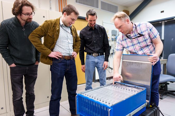
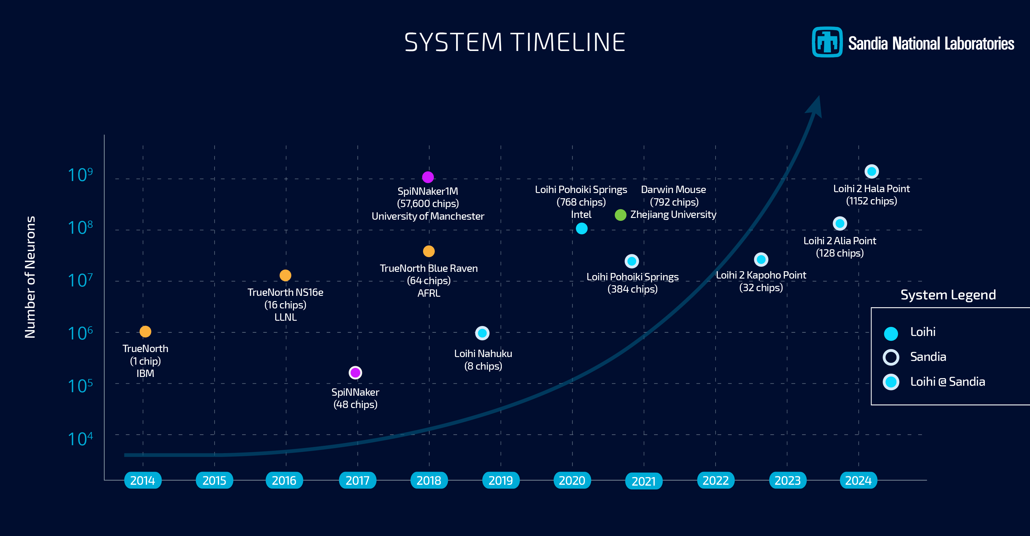
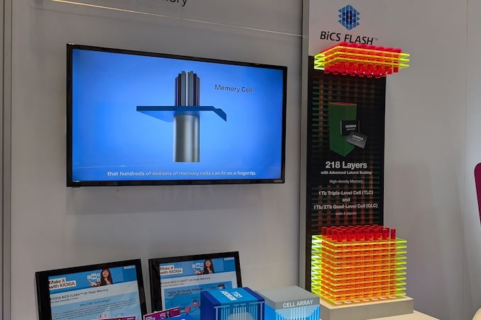
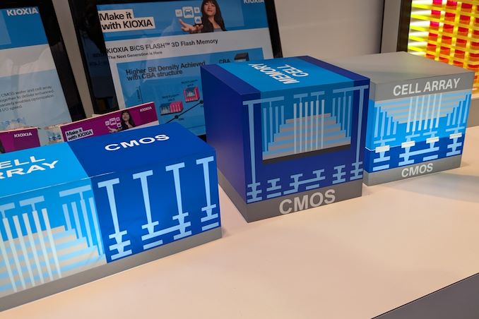
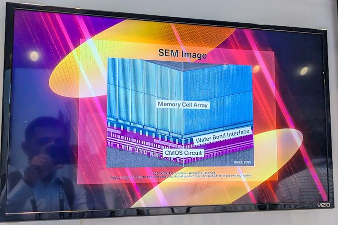
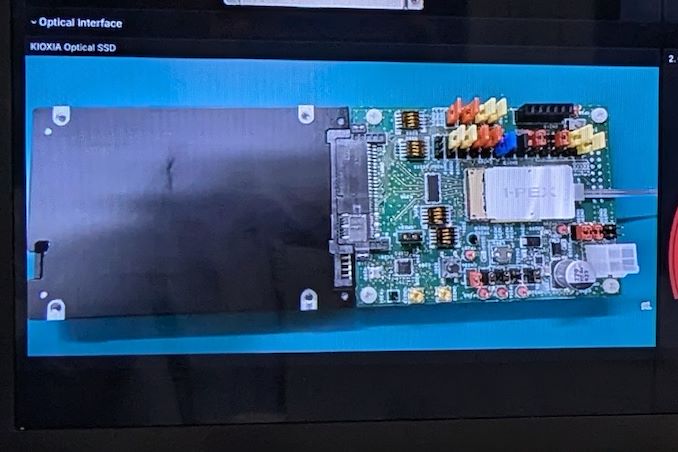
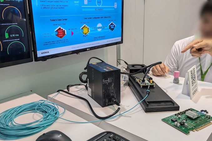
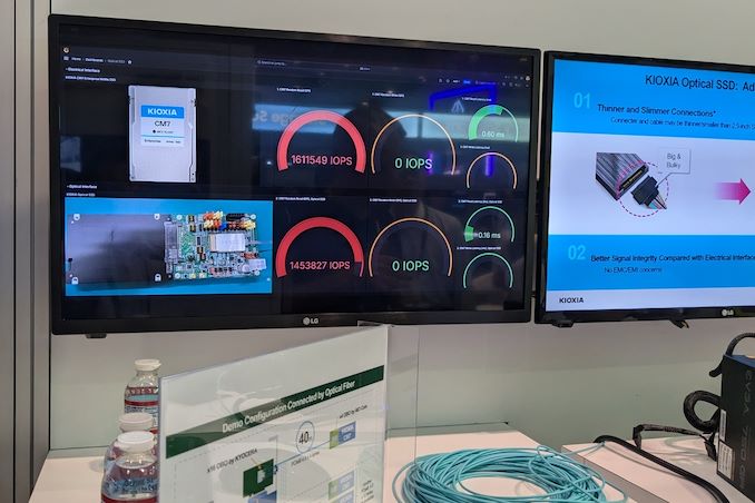


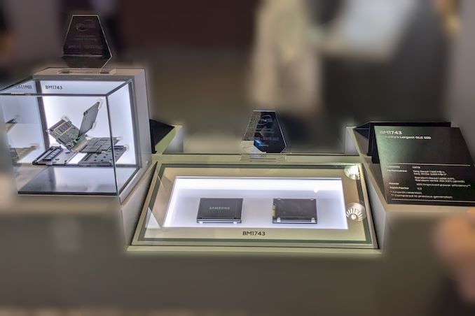
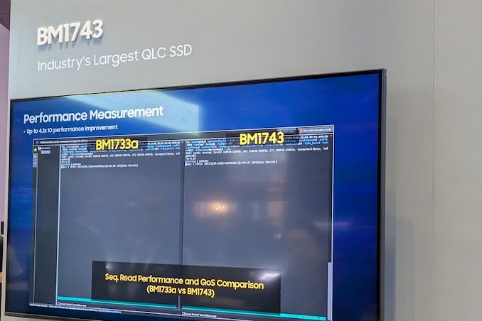
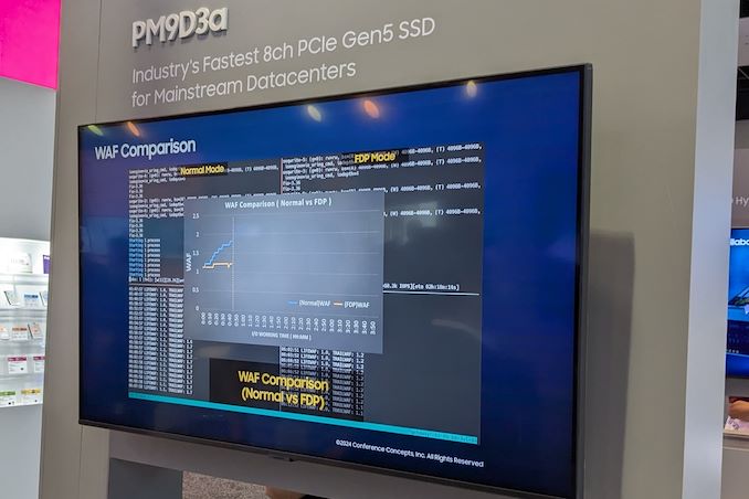
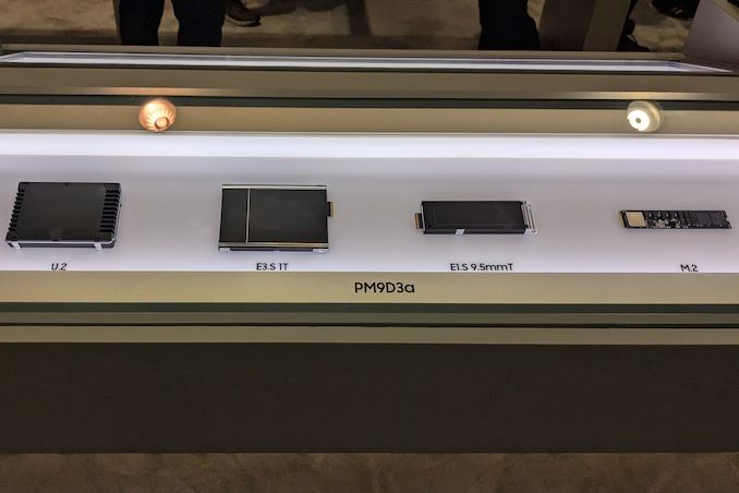
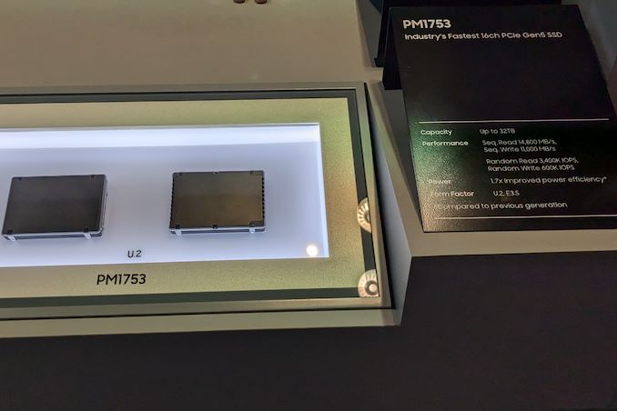
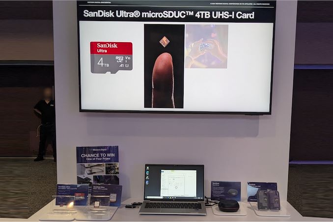
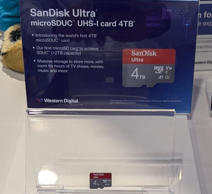
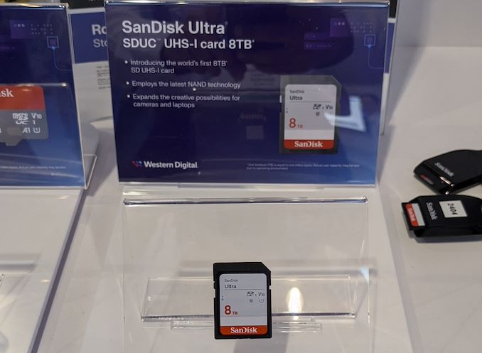
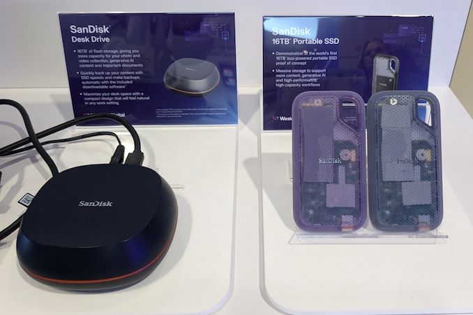

0 Comments