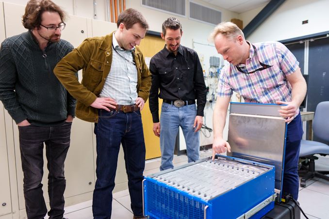

While neuromorphic computing remains under research for the time being, efforts into the field have continued to grow over the years, as have the capabilities of the specialty chips that have been developed for this research. Following those lines, this morning Intel and Sandia National Laboratories are celebrating the deployment of the Hala Point neuromorphic system, which the two believe is the highest capacity system in the world. With 1.15 billion neurons overall, Hala Point is the largest deployment yet for Intel’s Loihi 2 neuromorphic chip, which was first announced at the tail-end of 2021.
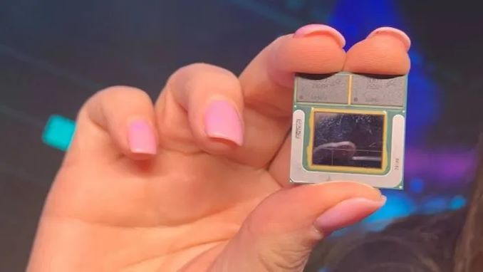
The Hala Point system incorporates 1152 Loihi 2 processors, each of which is capable of simulating a million neurons. As noted back at the time of Loihi 2’s launch, these chips are actually rather small – just 31 mm2 per chip with 2.3 billion transistors each, as they’re built on the Intel 4 process (one of the only other Intel chips to do so, besides Meteor Lake). As a result, the complete system is similarly petite, taking up just 6 rack units of space (or as Sandia likes to compare it to, about the size of a microwave), with a power consumption of 2.6 kW. Now that it’s online, Hala Point has dethroned the SpiNNaker system as the largest disclosed neuromorphic system, offering admittedly just a slightly larger number of neurons at less than 3% of the power consumption of the 100 kW British system.
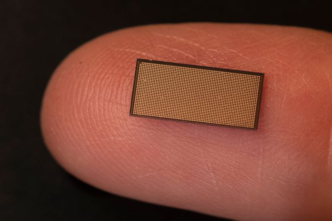
A Single Loihi 2 Chip (31 mm2)
Hala Point will be replacing an older Intel neuromorphic system at Sandia, Pohoiki Springs, which is based on Intel’s first-generation Loihi chips. By comparison, Hala Point offers ten-times as many neurons, and upwards of 12x the performance overall,
Both neuromorphic systems have been procured by Sandia in order to advance the national lab’s research into neuromorphic computing, a computing paradigm that behaves like a brain. The central thought (if you’ll excuse the pun) is that by mimicking the wetware writing this article, neuromorphic chips can be used to solve problems that conventional processors cannot solve today, and that they can do so more efficiently as well.
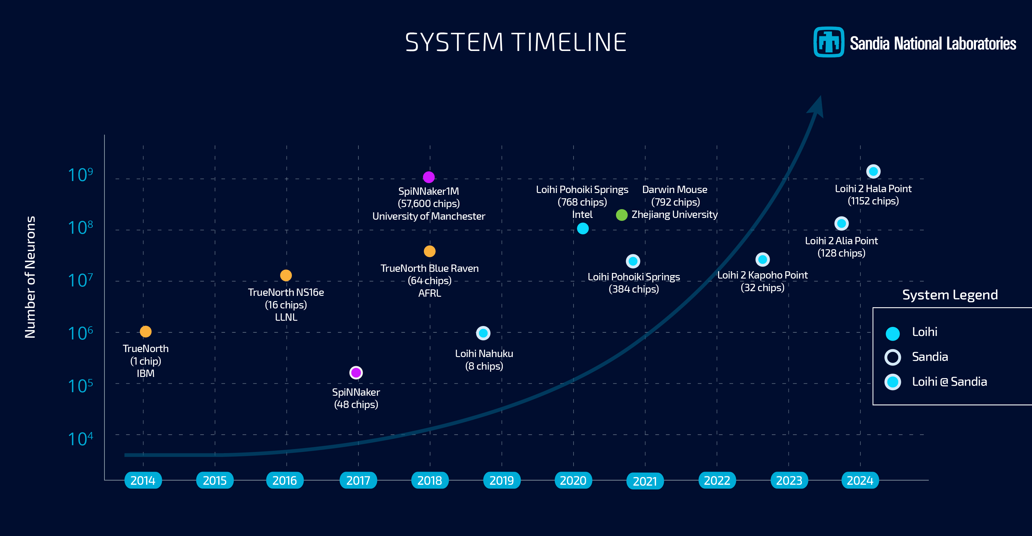
Sandia, for its part, has said that it will be using the system to look at large-scale neuromorphic computing, with work operating on a scale well beyond Pohoiki Springs. With Hala Point offering a simulated neuron count very roughly on the level of complexity of an owl brain, the lab believes that a larger-scale system will finally enable them to properly exploit the properties of neuromorphic computing to solve real problems in fields such as device physics, computer architecture, computer science and informatics, moving well beyond the simple demonstrations initially achieved at a smaller scale.
One new focus from the lab, which in turn has caught Intel’s attention, is the applicability of neuromorphic computing towards AI inference. Because the neural networks themselves behind the current wave of AI systems are attempting to emulate the human brain, in a sense, there is an obvious degree of synergy with the brain-mimicking neuromorphic chips, even if the algorithms differ in some key respects. Still, with energy efficiency being one of the major benefits of neuromorphic computing, it’s pushed Intel to look into the matter further – and even build a second, Hala Point-sized system of their own.
According to Intel, in their research on Hala Point, the system has reached efficiencies as high as 15 TOPS-per-Watt at 8-bit precision, albeit while using 10:1 sparsity, making it more than competitive with current-generation commercial chips. As an added bonus to that efficiency, the neuromorphic systems don’t require extensive data processing and batching in advance, which is normally necessary to make efficient use of the high density ALU arrays in GPUs and GPU-like processors.
Perhaps the most interesting use case of all, however, is the potent... CPUs

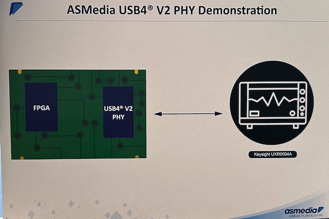
The USB Implementers Forum (USB-IF) introduced USB4 version 2.0 in fall 2022, and it expects systems and devices with the tech to emerge later this year and into next year. These upcoming products will largely rely on Intel's Barlow Ridge controller, a full-featured Thunderbolt 5 controller that goes above and beond the baseline USB4 v2 spec. And though extremely capable, Intel's Thunderbolt controllers are also quite expensive, and Barlow Ridge isn't expected to be any different. Fortunately, for system and device vendors that just need a basic USB4 v2 solution, ASMedia is also working on its own USB4 v2 controller.
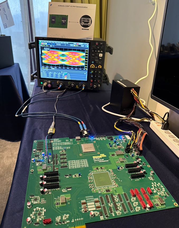
At Computex 2024, ASMedia demonstrated a prototype of its upcoming USB4 v2 physical interface (PHY), which will support USB4 v2's new Gen 4 (160Gbps) data rates and the associated PAM-3 signal encoding. The prototype was implemented using an FPGA, as the company yet has to tape out the completed controller.
Ultimately, the purpose of showing off a FPGA-based PHY at Computex was to allow ASMedia to demonstrate their current PHY design. With the shift to PAM-3 encoding for USB4 v2, ASMedia (and the rest of the USB ecosystem) must develop significantly more complex controllers – and there's no part of that more critical than a solid and reliable PHY design.
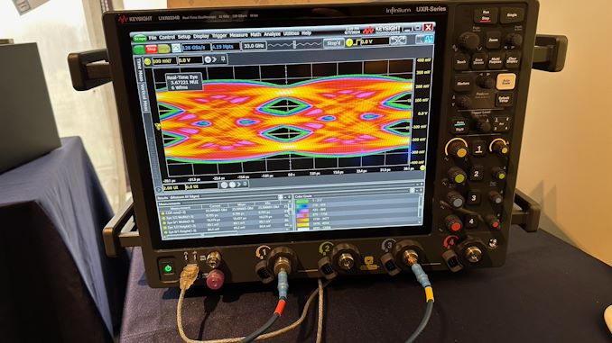
As part of their demonstration, ASMedia had a classic eye diagram display. The eye diagram demoed has a clear opening in the center, which is indicative of good signal integrity, as the larger the eye opening, the less distortion and noise in the signal. The horizontal width of the eye opening represents the time window in which the signal can be sampled correctly, so the relatively narrow horizontal spread of the eye opening suggests that there is minimal jitter, meaning the signal transitions are consistent and predictable. Finally, the vertical height of the eye opening indicates the signal amplitude and the rather tall eye opening suggests a higher signal-to-noise ratio (SNR), meaning that the signal is strong compared to any noise present.
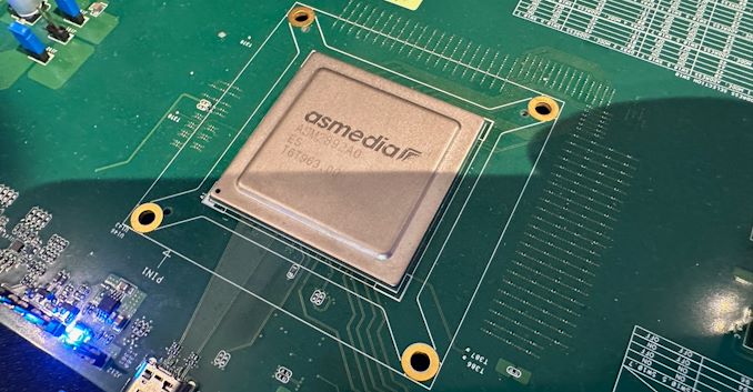
ASMedia itself is one of the major suppliers for discrete USB controllers, so the availability of ASMedia's USB4 v2 chip is crucial for adoption of the standard in general. While Intel will spearhead the industry with their Barlow Ridge Thunderbolt 5/USB4 v2 controller, ASMedia's controller is poised to end up in a far larger range of devices. So the importance of the company's USB4 v2 PHY demo is hard to overstate.
Demos aside, ASMedia is hoping to tape the chip out soon. If all goes well, the company expects their first USB4 v2 controllers to hit the market some time in the second half of 2025.
The USB Implementers Forum (USB-IF) introduced USB4 version 2.0 in fall 2022, and it expects systems and devices with the tech to emerge later this year and into next year. These upcoming products will largely rely on Intel's Barlow Ridge controller, a full-featured Thunderbolt 5 controller that goes above and beond the baseline USB4 v2 spec. And though extremely capable, Intel's Thunderbolt controllers are also quite expensive, and Barlow Ridge isn't expected to be any different. Fortunately, for system and device vendors that just need a basic USB4 v2 solution, ASMedia is also working on its own USB4 v2 controller.
At Computex 2024, ASMedia demonstrated a prototype of its upcoming USB4 v2 physical interface (PHY), which will support USB4 v2's new Gen 4 (160Gbps) data rates and the associated PAM-3 signal encoding. The prototype was implemented using an FPGA, as the company yet has to tape out the completed controller.
Ultimately, the purpose of showing off a FPGA-based PHY at Computex was to allow ASMedia to demonstrate their current PHY design. With the shift to PAM-3 encoding for USB4 v2, ASMedia (and the rest of the USB ecosystem) must develop significantly more complex controllers – and there's no part of that more critical than a solid and reliable PHY design.
As part of their demonstration, ASMedia had a classic eye diagram display. The eye diagram demoed has a clear opening in the center, which is indicative of good signal integrity, as the larger the eye opening, the less distortion and noise in the signal. The horizontal width of the eye opening represents the time window in which the signal can be sampled correctly, so the relatively narrow horizontal spread of the eye opening suggests that there is minimal jitter, meaning the signal transitions are consistent and predictable. Finally, the vertical height of the eye opening indicates the signal amplitude and the rather tall eye opening suggests a higher signal-to-noise ratio (SNR), meaning that the signal is strong compared to any noise present.
ASMedia itself is one of the major suppliers for discrete USB controllers, so the availability of ASMedia's USB4 v2 chip is crucial for adoption of the standard in general. While Intel will spearhead the industry with their Barlow Ridge Thunderbolt 5/USB4 v2 controller, ASMedia's controller is poised to end up in a far larger range of devices. So the importance of the company's USB4 v2 PHY demo is hard to overstate.
Demos aside, ASMedia is hoping to tape the chip out soon. If all goes well, the company expects their first USB4 v2 controllers to hit the market some time in the second half of 2025.

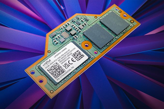
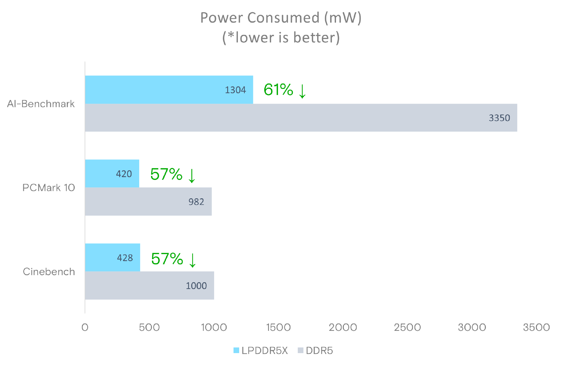
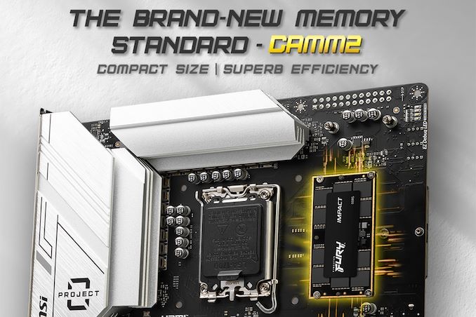
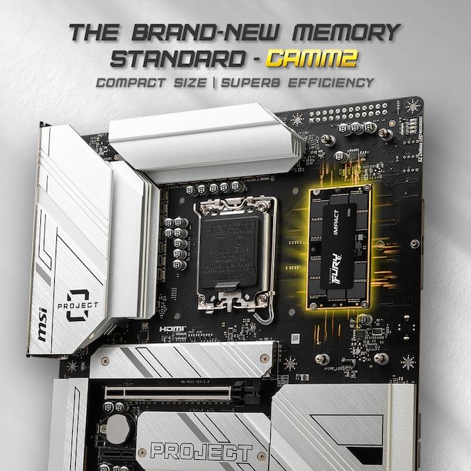
As LPCAMM2 adoption begins, the first retail memory modules are finally starting to hit the retail market, courtesy of Micron. The memory manufacturer has begun selling their LPDDR5X-based LPCAMM2 memory modules under their in-house Crucial brand, making them available on the latter's storefront. Timed to coincide with the release of Lenovo's ThinkPad P1 Gen 7 laptop – the first retail laptop designed to use the memory modules – this marks the de facto start of the eagerly-awaited modular LPDDR5X memory era.
Micron's Low Power Compression Attached Memory Module 2 (LPCAMM2) modules are available in capacities of 32 GB and 64 GB. These are dual-channel modules that feature a 128-bit wide interface, and are based around LPDDR5X memory running at data rates up to 7500 MT/s. This gives a single LPCAMM2 a peak bandwidth of 120 GB/s. Micron is not disclosing the latencies of its LPCAMM2 memory modules, but it says that high data transfer rates of LPDDR5X compensate for the extended timings.
Micron says that LPDDR5X memory offers significantly lower power consumption, with active power per 64-bit bus being 43-58% lower than DDR5 at the same speed, and standby power up to 80% lower. Meanwhile, similar to DDR5 modules, LPCAMM2 modules include a power management IC and voltage regulating circuitry, which provides module manufacturers additional opportunities to reduce power consumption of their products.
Source: Micron LPDDR5X LPCAMM2 Technical Brief
It's worth noting, however, that at least for the first generation of LPCAMM2 modules, system vendors will need to pick between modularity and performance. While soldered-down LPDDR5X memory is available at speeds up to 8533 MT/sec – and with 9600 MT/sec on the horizon – the fastest LPCAMM2 modules planned for this year by both Micron and rival Samsung will be running at 7500 MT/sec. So vendors will have to choose between the flexibility of offering modular LPDDR5X, or the higher bandwidth (and space savings) offered by soldering down their memory.
Micron, for its part, is projecting that 9600 MT/sec LPCAMM2 modules will be available by 2026. Though it's all but certain that faster memory will also be avaialble in the same timeframe.
Micron's Crucial LPDDR5X 32 GB module costs $174.99, whereas a 64 GB module costs $329.99.
Memory
Lorem Ipsum is simply dummy text of the printing and typesetting industry. Lorem Ipsum has been the industry's.


. As a result, the complete system is similarly petite, taking up just 6 rack units of space (or as Sandia likes to compare it to, about the size of a microwave), with a power consumption of 2.6 kW. Now that it’s online, Hala Point has dethroned <a href="http://apt.cs.manchester.ac.uk/projects/SpiNNaker/">the SpiNNaker system</a> as the largest disclosed neuromorphic system, offering admittedly just a slightly larger number of neurons at less than 3% of the power consumption of the 100 kW British system.</p>
<p align="center"><a href="https://www.anandtech.com/show/21355/intel-and-sandia-national-laboratories-roll-out-hala-point-neuromorphic-research-system"><img alt="" src="https://images.anandtech.com/doci/21355/LoihiFingertip3000_575px.jpg" /></a><br />
<small><em>A Single Loihi 2 Chip (31 mm<sup>2</sup>)</em></small></p>
<p>Hala Point will be replacing an older Intel neuromorphic system at Sandia, Pohoiki Springs, which is based on Intel’s first-generation Loihi chips. By comparison, Hala Point offers ten-times as many neurons, and upwards of 12x the performance overall,</p>
<p>Both neuromorphic systems have been procured by Sandia in order to advance the national lab’s research into neuromorphic computing, a computing paradigm that behaves like a brain. The central thought (if you’ll excuse the pun) is that by mimicking the wetware writing this article, neuromorphic chips can be used to solve problems that conventional processors cannot solve today, and that they can do so more efficiently as well.</p>
<p align="center"><a href="https://www.anandtech.com/show/21355/intel-and-sandia-national-laboratories-roll-out-hala-point-neuromorphic-research-system"><img alt="" src="https://images.anandtech.com/doci/21355/LOIHI_Chart-final.png" style="width: 100%;" /></a></p>
<p>Sandia, for its part, has said that it will be using the system to look at large-scale neuromorphic computing, with work operating on a scale well beyond Pohoiki Springs. With Hala Point offering a simulated neuron count very roughly on the level of complexity of an owl brain, the lab believes that a larger-scale system will finally enable them to properly exploit the properties of neuromorphic computing to solve real problems in fields such as device physics, computer architecture, computer science and informatics, moving well beyond the simple demonstrations initially achieved at a smaller scale.</p>
<p>One new focus from the lab, which in turn has caught Intel’s attention, is the applicability of neuromorphic computing towards AI inference. Because the neural networks themselves behind the current wave of AI systems are attempting to emulate the human brain, in a sense, there is an obvious degree of synergy with the brain-mimicking neuromorphic chips, even if the algorithms differ in some key respects. Still, with energy efficiency being one of the major benefits of neuromorphic computing, it’s pushed Intel to look into the matter further – and even build a second, Hala Point-sized system of their own.</p>
<p>According to Intel, in their research on Hala Point, the system has reached efficiencies as high as 15 TOPS-per-Watt at 8-bit precision, albeit while using 10:1 sparsity, making it more than competitive with current-generation commercial chips. As an added bonus to that efficiency, the neuromorphic systems don’t require extensive data processing and batching in advance, which is normally necessary to make efficient use of the high density ALU arrays in GPUs and GPU-like processors.</p>
<p>Perhaps the most interesting use case of all, however, is the potent... CPUs)
. As a result, the complete system is similarly petite, taking up just 6 rack units of space (or as Sandia likes to compare it to, about the size of a microwave), with a power consumption of 2.6 kW. Now that it’s online, Hala Point has dethroned <a href="http://apt.cs.manchester.ac.uk/projects/SpiNNaker/">the SpiNNaker system</a> as the largest disclosed neuromorphic system, offering admittedly just a slightly larger number of neurons at less than 3% of the power consumption of the 100 kW British system.</p>
<p align="center"><a href="https://www.anandtech.com/show/21355/intel-and-sandia-national-laboratories-roll-out-hala-point-neuromorphic-research-system"><img alt="" src="https://images.anandtech.com/doci/21355/LoihiFingertip3000_575px.jpg" /></a><br />
<small><em>A Single Loihi 2 Chip (31 mm<sup>2</sup>)</em></small></p>
<p>Hala Point will be replacing an older Intel neuromorphic system at Sandia, Pohoiki Springs, which is based on Intel’s first-generation Loihi chips. By comparison, Hala Point offers ten-times as many neurons, and upwards of 12x the performance overall,</p>
<p>Both neuromorphic systems have been procured by Sandia in order to advance the national lab’s research into neuromorphic computing, a computing paradigm that behaves like a brain. The central thought (if you’ll excuse the pun) is that by mimicking the wetware writing this article, neuromorphic chips can be used to solve problems that conventional processors cannot solve today, and that they can do so more efficiently as well.</p>
<p align="center"><a href="https://www.anandtech.com/show/21355/intel-and-sandia-national-laboratories-roll-out-hala-point-neuromorphic-research-system"><img alt="" src="https://images.anandtech.com/doci/21355/LOIHI_Chart-final.png" style="width: 100%;" /></a></p>
<p>Sandia, for its part, has said that it will be using the system to look at large-scale neuromorphic computing, with work operating on a scale well beyond Pohoiki Springs. With Hala Point offering a simulated neuron count very roughly on the level of complexity of an owl brain, the lab believes that a larger-scale system will finally enable them to properly exploit the properties of neuromorphic computing to solve real problems in fields such as device physics, computer architecture, computer science and informatics, moving well beyond the simple demonstrations initially achieved at a smaller scale.</p>
<p>One new focus from the lab, which in turn has caught Intel’s attention, is the applicability of neuromorphic computing towards AI inference. Because the neural networks themselves behind the current wave of AI systems are attempting to emulate the human brain, in a sense, there is an obvious degree of synergy with the brain-mimicking neuromorphic chips, even if the algorithms differ in some key respects. Still, with energy efficiency being one of the major benefits of neuromorphic computing, it’s pushed Intel to look into the matter further – and even build a second, Hala Point-sized system of their own.</p>
<p>According to Intel, in their research on Hala Point, the system has reached efficiencies as high as 15 TOPS-per-Watt at 8-bit precision, albeit while using 10:1 sparsity, making it more than competitive with current-generation commercial chips. As an added bonus to that efficiency, the neuromorphic systems don’t require extensive data processing and batching in advance, which is normally necessary to make efficient use of the high density ALU arrays in GPUs and GPU-like processors.</p>
<p>Perhaps the most interesting use case of all, however, is the potent... CPUs | https://compbuddey.blogspot.com/2024/04/intel-and-sandia-national-labs-roll-out_20.html)
. As a result, the complete system is similarly petite, taking up just 6 rack units of space (or as Sandia likes to compare it to, about the size of a microwave), with a power consumption of 2.6 kW. Now that it’s online, Hala Point has dethroned <a href="http://apt.cs.manchester.ac.uk/projects/SpiNNaker/">the SpiNNaker system</a> as the largest disclosed neuromorphic system, offering admittedly just a slightly larger number of neurons at less than 3% of the power consumption of the 100 kW British system.</p>
<p align="center"><a href="https://www.anandtech.com/show/21355/intel-and-sandia-national-laboratories-roll-out-hala-point-neuromorphic-research-system"><img alt="" src="https://images.anandtech.com/doci/21355/LoihiFingertip3000_575px.jpg" /></a><br />
<small><em>A Single Loihi 2 Chip (31 mm<sup>2</sup>)</em></small></p>
<p>Hala Point will be replacing an older Intel neuromorphic system at Sandia, Pohoiki Springs, which is based on Intel’s first-generation Loihi chips. By comparison, Hala Point offers ten-times as many neurons, and upwards of 12x the performance overall,</p>
<p>Both neuromorphic systems have been procured by Sandia in order to advance the national lab’s research into neuromorphic computing, a computing paradigm that behaves like a brain. The central thought (if you’ll excuse the pun) is that by mimicking the wetware writing this article, neuromorphic chips can be used to solve problems that conventional processors cannot solve today, and that they can do so more efficiently as well.</p>
<p align="center"><a href="https://www.anandtech.com/show/21355/intel-and-sandia-national-laboratories-roll-out-hala-point-neuromorphic-research-system"><img alt="" src="https://images.anandtech.com/doci/21355/LOIHI_Chart-final.png" style="width: 100%;" /></a></p>
<p>Sandia, for its part, has said that it will be using the system to look at large-scale neuromorphic computing, with work operating on a scale well beyond Pohoiki Springs. With Hala Point offering a simulated neuron count very roughly on the level of complexity of an owl brain, the lab believes that a larger-scale system will finally enable them to properly exploit the properties of neuromorphic computing to solve real problems in fields such as device physics, computer architecture, computer science and informatics, moving well beyond the simple demonstrations initially achieved at a smaller scale.</p>
<p>One new focus from the lab, which in turn has caught Intel’s attention, is the applicability of neuromorphic computing towards AI inference. Because the neural networks themselves behind the current wave of AI systems are attempting to emulate the human brain, in a sense, there is an obvious degree of synergy with the brain-mimicking neuromorphic chips, even if the algorithms differ in some key respects. Still, with energy efficiency being one of the major benefits of neuromorphic computing, it’s pushed Intel to look into the matter further – and even build a second, Hala Point-sized system of their own.</p>
<p>According to Intel, in their research on Hala Point, the system has reached efficiencies as high as 15 TOPS-per-Watt at 8-bit precision, albeit while using 10:1 sparsity, making it more than competitive with current-generation commercial chips. As an added bonus to that efficiency, the neuromorphic systems don’t require extensive data processing and batching in advance, which is normally necessary to make efficient use of the high density ALU arrays in GPUs and GPU-like processors.</p>
<p>Perhaps the most interesting use case of all, however, is the potent... CPUs&body=https://compbuddey.blogspot.com/2024/04/intel-and-sandia-national-labs-roll-out_20.html)
0 Comments