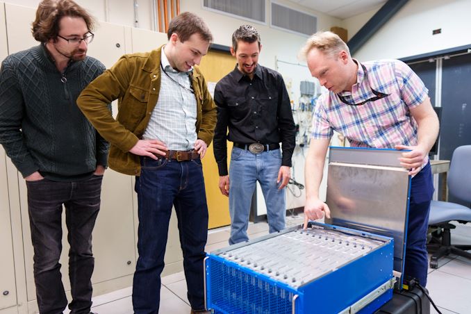

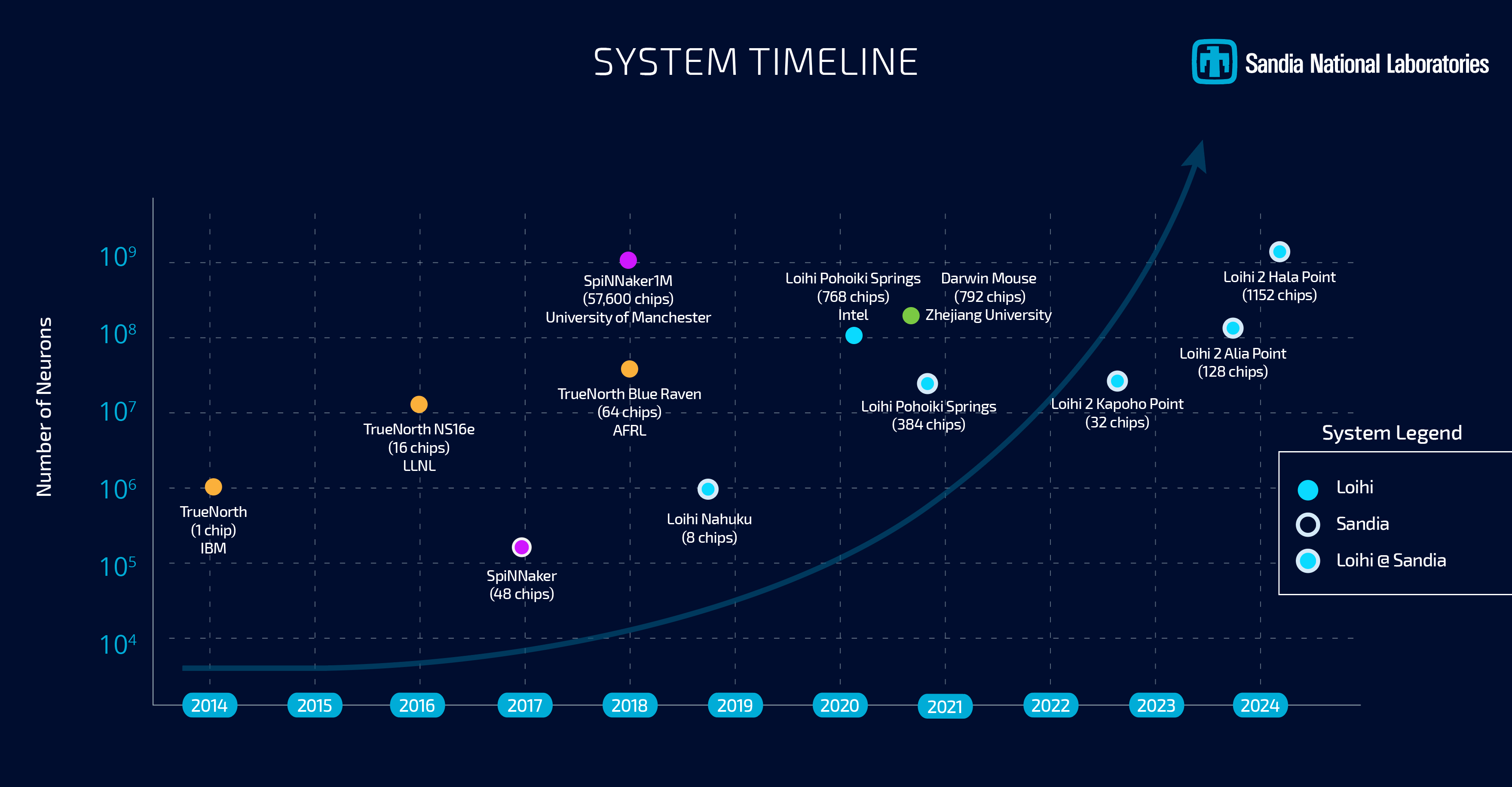
While neuromorphic computing remains under research for the time being, efforts into the field have continued to grow over the years, as have the capabilities of the specialty chips that have been developed for this research. Following those lines, this morning Intel and Sandia National Laboratories are celebrating the deployment of the Hala Point neuromorphic system, which the two believe is the highest capacity system in the world. With 1.15 billion neurons overall, Hala Point is the largest deployment yet for Intel’s Loihi 2 neuromorphic chip, which was first announced at the tail-end of 2021.
The Hala Point system incorporates 1152 Loihi 2 processors, each of which is capable of simulating a million neurons. As noted back at the time of Loihi 2’s launch, these chips are actually rather small – just 31 mm2 per chip with 2.3 billion transistors each, as they’re built on the Intel 4 process (one of the only other Intel chips to do so, besides Meteor Lake). As a result, the complete system is similarly petite, taking up just 6 rack units of space (or as Sandia likes to compare it to, about the size of a microwave), with a power consumption of 2.6 kW. Now that it’s online, Hala Point has dethroned the SpiNNaker system as the largest disclosed neuromorphic system, offering admittedly just a slightly larger number of neurons at less than 3% of the 100 kW British system.
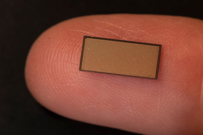
A Single Loihi 2 Chip (31 mm2)
Hala Point will be replacing an older Intel neuromorphic system at Sandia, Pohoiki Springs, which is based on Intel’s first-generation Loihi chips. By comparison, Hala Point offers ten-times as many neurons, and upwards of 12x the performance overall,
Both neuromorphic systems have been procured by Sandia in order to advance the national lab’s research into neuromorphic computing, a computing paradigm that behaves like a brain. The central thought (if you’ll excuse the pun) is that by mimicking the wetware writing this article, neuromorphic chips can be used to solve problems that conventional processors cannot solve today, and that they can do so more efficiently as well.
Sandia, for its part, has said that it will be using the system to look at large-scale neuromorphic computing, with work operating on a scale well beyond Pohoiki Springs. With Hala Point offering a simulated neuron count very roughly on the level of complexity of an owl brain, the lab believes that a larger-scale system will finally enable them to properly exploit the properties of neuromorphic computing to solve real problems in fields such as device physics, computer architecture, computer science and informatics, moving well beyond the simple demonstrations initially achieved at a smaller scale.
One new focus from the lab, which in turn has caught Intel’s attention, is the applicability of neuromorphic computing towards AI inference. Because the neural networks themselves behind the current wave of AI systems are attempting to emulate the human brain, in a sense, there is an obvious degree of synergy with the brain-mimicking neuromorphic chips, even if the algorithms differ in some key respects. Still, with energy efficiency being one of the major benefits of neuromorphic computing, it’s pushed Intel to look into the matter further – and even build a second, Hala Point-sized system of their own.
According to Intel, in their research on Hala Point, the system has reached efficiencies as high as 15 TOPS-per-Watt at 8-bit precision, albeit while using 10:1 sparsity, making it more than competitive with current-generation commercial chips. As an added bonus to that efficiency, the neuromorphic systems don’t require extensive data processing and batching in advance, which is normally necessary to make efficient use of the high density ALU arrays in GPUs and GPU-like processors.
Perhaps the most interesting use case of all, however, is the potential for being able to use... CPUs

Intel has divested its entire stake in Arm Holdings during the second quarter, raising approximately $147 million. Alongside this, Intel sold its stake in cybersecurity firm ZeroFox and reduced its holdings in Astera Labs, all as part of a broader effort to manage costs and recover cash amid significant financial challenges.
The sale of Intel's 1.18 million shares in Arm Holdings, as reported in a recent SEC filing, comes at a time when the company is struggling with substantial financial losses. Despite the $147 million generated from the sale, Intel reported a $120 million net loss on its equity investments for the quarter, which is a part of a larger $1.6 billion loss that Intel faced during this period.
In addition to selling its stake in Arm, Intel also exited its investment in ZeroFox and reduced its involvement with Astera Labs, a company known for developing connectivity platforms for enterprise hardware. These moves are in line with Intel's strategy to reduce costs and stabilize its financial position as it faces ongoing market challenges.
Despite the divestment, Intel's past investment in Arm was likely driven by strategic considerations. Arm Holdings is a significant force in the semiconductor industry, with its designs powering most mobile devices, and, for obvious reasons, Intel would like to address these. Intel and Arm are also collaborating on datacenter platforms tailored for Intel's 18A process technology. Additionally, Arm might view Intel as a potential licensee for its technologies and a valuable partner for other companies that license Arm's designs.
Intel's investment in Astera Labs was also a strategic one as the company probably wanted to secure steady supply of smart retimers, smart cable modems, and CXL memory controller, which are used in volumes in datacenters and Intel is certainly interested in selling as many datacenter CPUs as possible.
Intel's financial struggles were highlighted earlier this month when the company released a disappointing earnings report, which led to a 33% drop in its stock value, erasing billions of dollars of capitalization. To counter these difficulties, Intel announced plans to cut 15,000 jobs and implement other expense reductions. The company has also suspended its dividend, signaling the depth of its efforts to conserve cash and focus on recovery. When it comes to divestment of Arm stock, the need for immediate financial stabilization has presumably taken precedence, leading to the decision.
CPUs
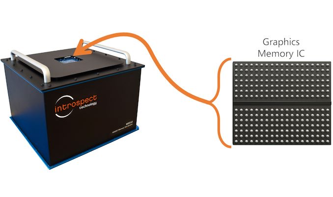
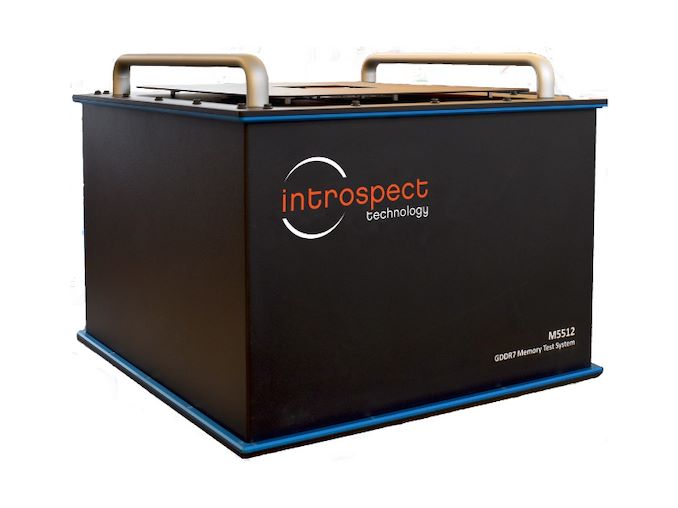
Introspect this week introduced its M5512 GDDR7 memory test system, which is designed for testing GDDR7 memory controllers, physical interface, and GDDR7 SGRAM chips. The tool will enable memory and processor manufacturers to verify that their products perform as specified by the standard.
One of the crucial phases of a processor design bring up is testing its standard interfaces, such as PCIe, DisplayPort, or GDDR is to ensure that they behave as specified both logically and electrically and achieve designated performance. Introspect's M5512 GDDR7 memory test system is designed to do just that: test new GDDR7 memory devices, troubleshoot protocol issues, assess signal integrity, and conduct comprehensive memory read/write stress tests.
The product will be quite useful for designers of GPUs/SoCs, graphics cards, PCs, network equipment and memory chips, which will speed up development of actual products that rely on GDDR7 memory. For now, GPU and SoC designers as well as memory makers use highly-custom setups consisting of many tools to characterize signal integrity as well as conduct detailed memory read/write functional stress testing, which are important things at this phase of development. But usage of a single tool greatly speeds up all the processes and gives a more comprehensive picture to specialists.
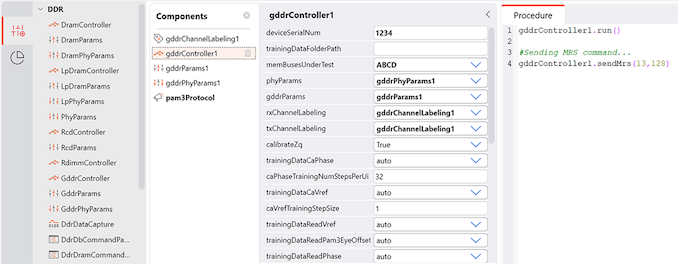
The M5512 GDDR7 Memory Test System is a desktop testing and measurement device that is equippped with 72 pins capable of functioning at up to 40 Gbps in PAM3 mode, as well as offering a virtual GDDR7 memory controller. The device features bidirectional circuitry for executing read and write operations, and every pin is equipped with an extensive range of analog characterization features, such as skew injection with femto-second resolution, voltage control with millivolt resolution, programmable jitter injection, and various eye margining features critical for AC characterization and conformance testing. Furthermore, the system integrates device power supplies with precise power sequencing and ramping controls, providing a comprehensive solution for both AC characterization and memory functional stress testing on any GDDR7 device.
Introspects M5512 has been designed in close collaboration with JEDEC members working on the GDDR7 specification, so it promises to meet all of their requirements for compliance testing. Notably, however, the device does not eliminate need for interoperability tests and still requires companies to develop their own test algorithms, but it's still a significant tool for bootstrapping device development and getting it to the point where chips can begin interop testing.
“In its quest to support the industry on GDDR7 deployment, Introspect Technology has worked tirelessly in the last few years with JEDEC members to develop the M5512 GDDR7 Memory Test System,” said Dr. Mohamed Hafed, CEO at Introspect Technology.
GPUs
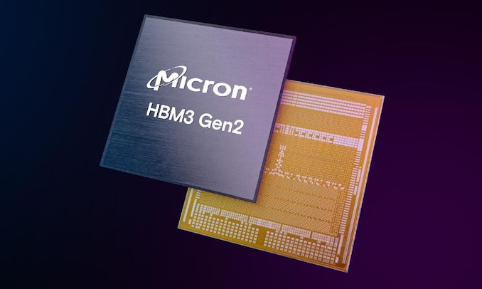
Being the first company to ship HBM3E memory has its perks for Micron, as the company has revealed that is has managed to sell out the entire supply of its advanced high-bandwidth memory for 2024, while most of their 2025 production has been allocated, as well. Micron's HBM3E memory (or how Micron alternatively calls it, HBM3 Gen2) was one of the first to be qualified for NVIDIA's updated H200/GH200 accelerators, so it looks like the DRAM maker will be a key supplier to the green company.
"Our HBM is sold out for calendar 2024, and the overwhelming majority of our 2025 supply has already been allocated," said Sanjay Mehrotra, chief executive of Micron, in prepared remarks for the company's earnings call this week. "We continue to expect HBM bit share equivalent to our overall DRAM bit share sometime in calendar 2025."
Micron's first HBM3E product is an 8-Hi 24 GB stack with a 1024-bit interface, 9.2 GT/s data transfer rate, and a total bandwidth of 1.2 TB/s. NVIDIA's H200 accelerator for artificial intelligence and high-performance computing will use six of these cubes, providing a total of 141 GB of accessible high-bandwidth memory.
"We are on track to generate several hundred million dollars of revenue from HBM in fiscal 2024 and expect HBM revenues to be accretive to our DRAM and overall gross margins starting in the fiscal third quarter," said Mehrotra.
The company has also began sampling its 12-Hi 36 GB stacks that offer a 50% more capacity. These KGSDs will ramp in 2025 and will be used for next generations of AI products. Meanwhile, it does not look like NVIDIA's B100 and B200 are going to use 36 GB HBM3E stacks, at least initially.
Demand for artificial intelligence servers set records last year, and it looks like it is going to remain high this year as well. Some analysts believe that NVIDIA's A100 and H100 processors (as well as their various derivatives) commanded as much as 80% of the entire AI processor market in 2023. And while this year NVIDIA will face tougher competition from AMD, AWS, D-Matrix, Intel, Tenstorrent, and other companies on the inference front, it looks like NVIDIA's H200 will still be the processor of choice for AI training, especially for big players like Meta and Microsoft, who already run fleets consisting of hundreds of thousands of NVIDIA accelerators. With that in mind, being a primary supplier of HBM3E for NVIDIA's H200 is a big deal for Micron as it enables it to finally capture a sizeable chunk of the HBM market, which is currently dominated by SK Hynix and Samsung, and where Micron controlled only about 10% as of last year.
Meanwhile, since every DRAM device inside an HBM stack has a wide interface, it is physically bigger than regular DDR4 or DDR5 ICs. As a result, the ramp of HBM3E memory will affect bit supply of commodity DRAMs from Micron, the company said.
"The ramp of HBM production will constrain supply growth in non-HBM products," Mehrotra said. "Industrywide, HBM3E consumes approximately three times the wafer supply as DDR5 to produce a given number of bits in the same technology node."
Memory

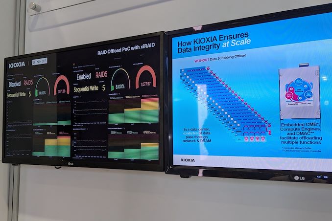
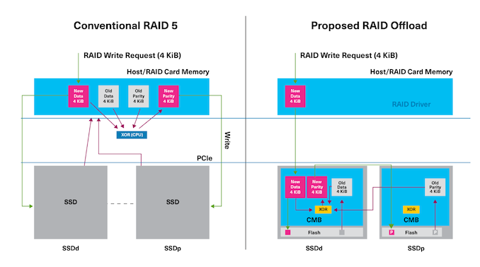
Kioxia's booth at FMS 2024 was a busy one with multiple technology demonstrations keeping visitors occupied. A walk-through of the BiCS 8 manufacturing process was the first to grab my attention. Kioxia and Western Digital announced the sampling of BiCS 8 in March 2023. We had touched briefly upon its CMOS Bonded Array (CBA) scheme in our coverage of Kioxial's 2Tb QLC NAND device and coverage of Western Digital's 128 TB QLC enterprise SSD proof-of-concept demonstration. At Kioxia's booth, we got more insights.

Traditionally, fabrication of flash chips involved placement of the associate logic circuitry (CMOS process) around the periphery of the flash array. The process then moved on to putting the CMOS under the cell array, but the wafer development process was serialized with the CMOS logic getting fabricated first followed by the cell array on top. However, this has some challenges because the cell array requires a high-temperature processing step to ensure higher reliability that can be detrimental to the health of the CMOS logic. Thanks to recent advancements in wafer bonding techniques, the new CBA process allows the CMOS wafer and cell array wafer to be processed independently in parallel and then pieced together, as shown in the models above.

The BiCS 8 3D NAND incorporates 218 layers, compared to 112 layers in BiCS 5 and 162 layers in BiCS 6. The company decided to skip over BiCS 7 (or, rather, it was probably a short-lived generation meant as an internal test vehicle). The generation retains the four-plane charge trap structure of BiCS 6. In its TLC avatar, it is available as a 1 Tbit device. The QLC version is available in two capacities - 1 Tbit and 2 Tbit.
Kioxia also noted that while the number of layers (218) doesn't compare favorably with the latest layer counts from the competition, its lateral scaling / cell shrinkage has enabled it to be competitive in terms of bit density as well as operating speeds (3200 MT/s). For reference, the latest shipping NAND from Micron - the G9 - has 276 layers with a bit density in TLC mode of 21 Gbit/mm2, and operates at up to 3600 MT/s. However, its 232L NAND operates only up to 2400 MT/s and has a bit density of 14.6 Gbit/mm2.
It must be noted that the CBA hybrid bonding process has advantages over the current processes used by other vendors - including Micron's CMOS under array (CuA) and SK hynix's 4D PUC (periphery-under-chip) developed in the late 2010s. It is expected that other NAND vendors will also move eventually to some variant of the hybrid bonding scheme used by Kioxia.
Storage
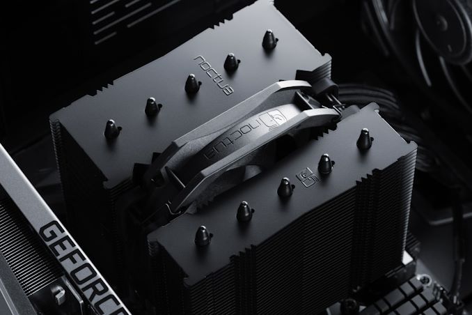
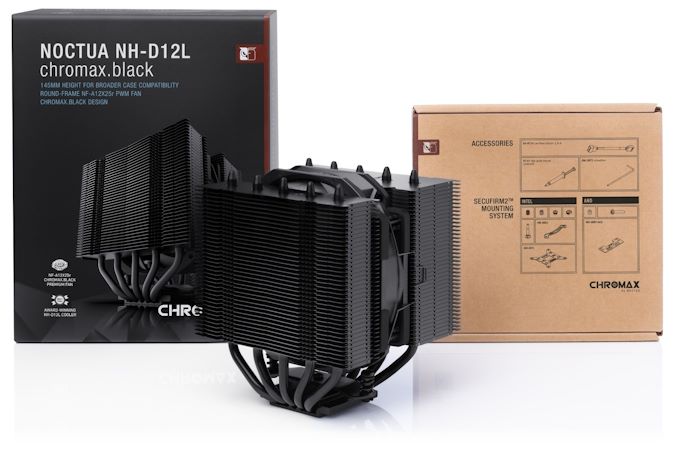
Today, Noctua announced the launch of its NH-D12L chromax.black CPU cooler, an all-black version of the existing NH-D12L. The cooler sports not only a coat of mattte black paint, but also a relatively short height of 145mm, which Noctua says makes the NH-D12L suitable for slimmer cases and 4U server racks.
Having launched in 2022, the NH-D12L is essentially a shorter version of the NH-U12A, which stands at 158mm tall. While plenty of cases have the room for a cooler that tall, not all do (especially small form factor cases). The NH-D12L exists to offer similar performance as the NH-U12A but for cases where 145mm would fit but 158mm wouldn’t. However, the NH-D12L has just a single 120mm NF-A12x25 fan, whereas the NH-U12A has two. Additionally, the NH-D12L has five heatpipes to the NH-U12A’s seven. These two factors mean the NH-D12L can’t quite catch up to the NH-U12A when it comes to cooling capacity.
The chromax.black model is practically identical to the original, but features Noctua’s popular black motif. It should perform the same, and its SecuFirm 2 mounting hardware supports the same sockets: AMD’s AM4 and AM5, and Intel’s LGA 1700 and LGA 1851 for upcoming Arrow Lake CPUs. Despite its compact design, the NH-D12L also has “100% RAM compatibility” for sticks with tall heatspreaders, which sometimes pose clearance issues with air coolers.
The NH-D12L chromax.black also comes with the usual Noctua accessories: a screwdriver, NH-T1 thermal paste, and a four-pin low-noise adapter for the NF-A12x25 fan. Additionally, the 120mm fan is mounted to the cooler via a bracket, meaning no screws are necessary and it can be removed or installed toollessly.
At $99/€109, the NH-D12L is positioned fairly high in the market, next to larger high-end air coolers such as Corsair’s A115, as well as 240mm to 360mm AIO liquid coolers. However, the NH-D12L holds a substantial advantage in its size and compatibility, and while many of these high-end air coolers are 160mm tall or more, the NH-D12L is just 145mm. In some cases, even 15mm could make a big difference.
CPU cooler

A few years back, the Japanese government's New Energy and Industrial Technology Development Organization (NEDO ) allocated funding for the development of green datacenter technologies. With the aim to obtain up to 40% savings in overall power consumption, several Japanese companies have been developing an optical interface for their enterprise SSDs. And at this year's FMS, Kioxia had their optical interface on display.

For this demonstration, Kioxia took its existing CM7 enterprise SSD and created an optical interface for it. A PCIe card with on-board optics developed by Kyocera is installed in the server slot. An optical interface allows data transfer over long distances (it was 40m in the demo, but Kioxia promises lengths of up to 100m for the cable in the future). This allows the storage to be kept in a separate room with minimal cooling requirements compared to the rack with the CPUs and GPUs. Disaggregation of different server components will become an option as very high throughput interfaces such as PCIe 7.0 (with 128 GT/s rates) become available.

The demonstration of the optical SSD showed a slight loss in IOPS performance, but a significant advantage in the latency metric over the shipping enterprise SSD behind a copper network link. Obviously, there are advantages in wiring requirements and signal integrity maintenance with optical links.
Being a proof-of-concept demonstration, we do see the requirement for an industry-standard approach if this were to gain adoption among different datacenter vendors. The PCI-SIG optical workgroup will need to get its act together soon to create a standards-based approach to this problem.
Storage
Introspect this week introduced its M5512 GDDR7 memory test system, which is designed for testing GDDR7 memory controllers, physical interface, and GDDR7 SGRAM chips. The tool will enable memory and processor manufacturers to verify that their products perform as specified by the standard.
One of the crucial phases of a processor design bring up is testing its standard interfaces, such as PCIe, DisplayPort, or GDDR is to ensure that they behave as specified both logically and electrically and achieve designated performance. Introspect's M5512 GDDR7 memory test system is designed to do just that: test new GDDR7 memory devices, troubleshoot protocol issues, assess signal integrity, and conduct comprehensive memory read/write stress tests.
The product will be quite useful for designers of GPUs/SoCs, graphics cards, PCs, network equipment and memory chips, which will speed up development of actual products that rely on GDDR7 memory. For now, GPU and SoC designers as well as memory makers use highly-custom setups consisting of many tools to characterize signal integrity as well as conduct detailed memory read/write functional stress testing, which are important things at this phase of development. But usage of a single tool greatly speeds up all the processes and gives a more comprehensive picture to specialists.
The M5512 GDDR7 Memory Test System is a desktop testing and measurement device that is equippped with 72 pins capable of functioning at up to 40 Gbps in PAM3 mode, as well as offering a virtual GDDR7 memory controller. The device features bidirectional circuitry for executing read and write operations, and every pin is equipped with an extensive range of analog characterization features, such as skew injection with femto-second resolution, voltage control with millivolt resolution, programmable jitter injection, and various eye margining features critical for AC characterization and conformance testing. Furthermore, the system integrates device power supplies with precise power sequencing and ramping controls, providing a comprehensive solution for both AC characterization and memory functional stress testing on any GDDR7 device.
Introspects M5512 has been designed in close collaboration with JEDEC members working on the GDDR7 specification, so it promises to meet all of their requirements for compliance testing. Notably, however, the device does not eliminate need for interoperability tests and still requires companies to develop their own test algorithms, but it's still a significant tool for bootstrapping device development and getting it to the point where chips can begin interop testing.
“In its quest to support the industry on GDDR7 deployment, Introspect Technology has worked tirelessly in the last few years with JEDEC members to develop the M5512 GDDR7 Memory Test System,” said Dr. Mohamed Hafed, CEO at Introspect Technology.
GPUs
Lorem Ipsum is simply dummy text of the printing and typesetting industry. Lorem Ipsum has been the industry's.
Intel has divested its entire stake in Arm Holdings during the second quarter, raising approximately $147 million. Alongside this, Intel sold its stake in cybersecurity firm ZeroFox and reduced its holdings in Astera Labs, all as part of a broader effort to manage costs and recover cash amid significant financial challenges.
The sale of Intel's 1.18 million shares in Arm Holdings, as reported in a recent SEC filing, comes at a time when the company is struggling with substantial financial losses. Despite the $147 million generated from the sale, Intel reported a $120 million net loss on its equity investments for the quarter, which is a part of a larger $1.6 billion loss that Intel faced during this period.
In addition to selling its stake in Arm, Intel also exited its investment in ZeroFox and reduced its involvement with Astera Labs, a company known for developing connectivity platforms for enterprise hardware. These moves are in line with Intel's strategy to reduce costs and stabilize its financial position as it faces ongoing market challenges.
Despite the divestment, Intel's past investment in Arm was likely driven by strategic considerations. Arm Holdings is a significant force in the semiconductor industry, with its designs powering most mobile devices, and, for obvious reasons, Intel would like to address these. Intel and Arm are also collaborating on datacenter platforms tailored for Intel's 18A process technology. Additionally, Arm might view Intel as a potential licensee for its technologies and a valuable partner for other companies that license Arm's designs.
Intel's investment in Astera Labs was also a strategic one as the company probably wanted to secure steady supply of smart retimers, smart cable modems, and CXL memory controller, which are used in volumes in datacenters and Intel is certainly interested in selling as many datacenter CPUs as possible.
Intel's financial struggles were highlighted earlier this month when the company released a disappointing earnings report, which led to a 33% drop in its stock value, erasing billions of dollars of capitalization. To counter these difficulties, Intel announced plans to cut 15,000 jobs and implement other expense reductions. The company has also suspended its dividend, signaling the depth of its efforts to conserve cash and focus on recovery. When it comes to divestment of Arm stock, the need for immediate financial stabilization has presumably taken precedence, leading to the decision.
CPUs
. As a result, the complete system is similarly petite, taking up just 6 rack units of space (or as Sandia likes to compare it to, about the size of a microwave), with a power consumption of 2.6 kW. Now that it’s online, Hala Point has dethroned <a href="http://apt.cs.manchester.ac.uk/projects/SpiNNaker/">the SpiNNaker system</a> as the largest disclosed neuromorphic system, offering admittedly just a slightly larger number of neurons at less than 3% of the 100 kW British system.</p>
<p align="center"><a href="https://www.anandtech.com/show/21355/intel-and-sandia-national-laboratories-roll-out-hala-point-neuromorphic-research-system"><img alt="" src="https://images.anandtech.com/doci/21355/LoihiFingertip3000_575px.jpg" /></a><br />
<small><em>A Single Loihi 2 Chip (31 mm<sup>2</sup>)</em></small></p>
<p>Hala Point will be replacing an older Intel neuromorphic system at Sandia, Pohoiki Springs, which is based on Intel’s first-generation Loihi chips. By comparison, Hala Point offers ten-times as many neurons, and upwards of 12x the performance overall,</p>
<p>Both neuromorphic systems have been procured by Sandia in order to advance the national lab’s research into neuromorphic computing, a computing paradigm that behaves like a brain. The central thought (if you’ll excuse the pun) is that by mimicking the wetware writing this article, neuromorphic chips can be used to solve problems that conventional processors cannot solve today, and that they can do so more efficiently as well.</p>
<p align="center"><a href="https://www.anandtech.com/show/21355/intel-and-sandia-national-laboratories-roll-out-hala-point-neuromorphic-research-system"><img alt="" src="https://images.anandtech.com/doci/21355/LOIHI_Chart-final.png" style="width: 100%;" /></a></p>
<p>Sandia, for its part, has said that it will be using the system to look at large-scale neuromorphic computing, with work operating on a scale well beyond Pohoiki Springs. With Hala Point offering a simulated neuron count very roughly on the level of complexity of an owl brain, the lab believes that a larger-scale system will finally enable them to properly exploit the properties of neuromorphic computing to solve real problems in fields such as device physics, computer architecture, computer science and informatics, moving well beyond the simple demonstrations initially achieved at a smaller scale.</p>
<p>One new focus from the lab, which in turn has caught Intel’s attention, is the applicability of neuromorphic computing towards AI inference. Because the neural networks themselves behind the current wave of AI systems are attempting to emulate the human brain, in a sense, there is an obvious degree of synergy with the brain-mimicking neuromorphic chips, even if the algorithms differ in some key respects. Still, with energy efficiency being one of the major benefits of neuromorphic computing, it’s pushed Intel to look into the matter further – and even build a second, Hala Point-sized system of their own.</p>
<p>According to Intel, in their research on Hala Point, the system has reached efficiencies as high as 15 TOPS-per-Watt at 8-bit precision, albeit while using 10:1 sparsity, making it more than competitive with current-generation commercial chips. As an added bonus to that efficiency, the neuromorphic systems don’t require extensive data processing and batching in advance, which is normally necessary to make efficient use of the high density ALU arrays in GPUs and GPU-like processors.</p>
<p>Perhaps the most interesting use case of all, however, is the potential for being able to use... CPUs)
. As a result, the complete system is similarly petite, taking up just 6 rack units of space (or as Sandia likes to compare it to, about the size of a microwave), with a power consumption of 2.6 kW. Now that it’s online, Hala Point has dethroned <a href="http://apt.cs.manchester.ac.uk/projects/SpiNNaker/">the SpiNNaker system</a> as the largest disclosed neuromorphic system, offering admittedly just a slightly larger number of neurons at less than 3% of the 100 kW British system.</p>
<p align="center"><a href="https://www.anandtech.com/show/21355/intel-and-sandia-national-laboratories-roll-out-hala-point-neuromorphic-research-system"><img alt="" src="https://images.anandtech.com/doci/21355/LoihiFingertip3000_575px.jpg" /></a><br />
<small><em>A Single Loihi 2 Chip (31 mm<sup>2</sup>)</em></small></p>
<p>Hala Point will be replacing an older Intel neuromorphic system at Sandia, Pohoiki Springs, which is based on Intel’s first-generation Loihi chips. By comparison, Hala Point offers ten-times as many neurons, and upwards of 12x the performance overall,</p>
<p>Both neuromorphic systems have been procured by Sandia in order to advance the national lab’s research into neuromorphic computing, a computing paradigm that behaves like a brain. The central thought (if you’ll excuse the pun) is that by mimicking the wetware writing this article, neuromorphic chips can be used to solve problems that conventional processors cannot solve today, and that they can do so more efficiently as well.</p>
<p align="center"><a href="https://www.anandtech.com/show/21355/intel-and-sandia-national-laboratories-roll-out-hala-point-neuromorphic-research-system"><img alt="" src="https://images.anandtech.com/doci/21355/LOIHI_Chart-final.png" style="width: 100%;" /></a></p>
<p>Sandia, for its part, has said that it will be using the system to look at large-scale neuromorphic computing, with work operating on a scale well beyond Pohoiki Springs. With Hala Point offering a simulated neuron count very roughly on the level of complexity of an owl brain, the lab believes that a larger-scale system will finally enable them to properly exploit the properties of neuromorphic computing to solve real problems in fields such as device physics, computer architecture, computer science and informatics, moving well beyond the simple demonstrations initially achieved at a smaller scale.</p>
<p>One new focus from the lab, which in turn has caught Intel’s attention, is the applicability of neuromorphic computing towards AI inference. Because the neural networks themselves behind the current wave of AI systems are attempting to emulate the human brain, in a sense, there is an obvious degree of synergy with the brain-mimicking neuromorphic chips, even if the algorithms differ in some key respects. Still, with energy efficiency being one of the major benefits of neuromorphic computing, it’s pushed Intel to look into the matter further – and even build a second, Hala Point-sized system of their own.</p>
<p>According to Intel, in their research on Hala Point, the system has reached efficiencies as high as 15 TOPS-per-Watt at 8-bit precision, albeit while using 10:1 sparsity, making it more than competitive with current-generation commercial chips. As an added bonus to that efficiency, the neuromorphic systems don’t require extensive data processing and batching in advance, which is normally necessary to make efficient use of the high density ALU arrays in GPUs and GPU-like processors.</p>
<p>Perhaps the most interesting use case of all, however, is the potential for being able to use... CPUs | https://compbuddey.blogspot.com/2024/04/intel-and-sandia-national-labs-roll-out.html)
. As a result, the complete system is similarly petite, taking up just 6 rack units of space (or as Sandia likes to compare it to, about the size of a microwave), with a power consumption of 2.6 kW. Now that it’s online, Hala Point has dethroned <a href="http://apt.cs.manchester.ac.uk/projects/SpiNNaker/">the SpiNNaker system</a> as the largest disclosed neuromorphic system, offering admittedly just a slightly larger number of neurons at less than 3% of the 100 kW British system.</p>
<p align="center"><a href="https://www.anandtech.com/show/21355/intel-and-sandia-national-laboratories-roll-out-hala-point-neuromorphic-research-system"><img alt="" src="https://images.anandtech.com/doci/21355/LoihiFingertip3000_575px.jpg" /></a><br />
<small><em>A Single Loihi 2 Chip (31 mm<sup>2</sup>)</em></small></p>
<p>Hala Point will be replacing an older Intel neuromorphic system at Sandia, Pohoiki Springs, which is based on Intel’s first-generation Loihi chips. By comparison, Hala Point offers ten-times as many neurons, and upwards of 12x the performance overall,</p>
<p>Both neuromorphic systems have been procured by Sandia in order to advance the national lab’s research into neuromorphic computing, a computing paradigm that behaves like a brain. The central thought (if you’ll excuse the pun) is that by mimicking the wetware writing this article, neuromorphic chips can be used to solve problems that conventional processors cannot solve today, and that they can do so more efficiently as well.</p>
<p align="center"><a href="https://www.anandtech.com/show/21355/intel-and-sandia-national-laboratories-roll-out-hala-point-neuromorphic-research-system"><img alt="" src="https://images.anandtech.com/doci/21355/LOIHI_Chart-final.png" style="width: 100%;" /></a></p>
<p>Sandia, for its part, has said that it will be using the system to look at large-scale neuromorphic computing, with work operating on a scale well beyond Pohoiki Springs. With Hala Point offering a simulated neuron count very roughly on the level of complexity of an owl brain, the lab believes that a larger-scale system will finally enable them to properly exploit the properties of neuromorphic computing to solve real problems in fields such as device physics, computer architecture, computer science and informatics, moving well beyond the simple demonstrations initially achieved at a smaller scale.</p>
<p>One new focus from the lab, which in turn has caught Intel’s attention, is the applicability of neuromorphic computing towards AI inference. Because the neural networks themselves behind the current wave of AI systems are attempting to emulate the human brain, in a sense, there is an obvious degree of synergy with the brain-mimicking neuromorphic chips, even if the algorithms differ in some key respects. Still, with energy efficiency being one of the major benefits of neuromorphic computing, it’s pushed Intel to look into the matter further – and even build a second, Hala Point-sized system of their own.</p>
<p>According to Intel, in their research on Hala Point, the system has reached efficiencies as high as 15 TOPS-per-Watt at 8-bit precision, albeit while using 10:1 sparsity, making it more than competitive with current-generation commercial chips. As an added bonus to that efficiency, the neuromorphic systems don’t require extensive data processing and batching in advance, which is normally necessary to make efficient use of the high density ALU arrays in GPUs and GPU-like processors.</p>
<p>Perhaps the most interesting use case of all, however, is the potential for being able to use... CPUs&body=https://compbuddey.blogspot.com/2024/04/intel-and-sandia-national-labs-roll-out.html)
0 Comments