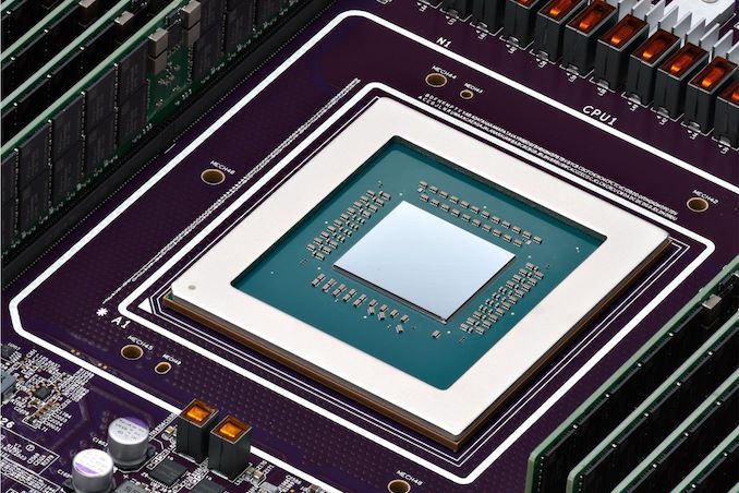

Google was among the first hyperscalers build custom silicon for its services, starting first with tensor processing units (TPUs) for its AI initiatives, and then video transcoding units (VCUs) for the YouTube service. But unlike its industry peers, the company has been slower to adopt custom CPU designs, prefering to stick to off-the-shelf chips from the major CPUs. This is finally changing at Google, with the announcement that the company has developed its own in-house datacenter CPU, the Axion.
Google's Axion processor is based on the Arm Neoverse V2 (Arm v9) platform, which is Arm's current-generation design for high-performance server CPUs, and is already employed in other chips such as NVIDIA's Grace and Amazon's Graviton4. Within Google, Axion is aimed at a wide variety of workloads, including web and app servers, data analytics, microservices, and AI training. Google claims that the Axion processors boast up to 50% higher performance and up to 60% better energy efficiency compared to current-generation x86-based processors, as well as offer a 30% higher performance compared to competing Arm-based CPUs for datacenters. Though as is increasingly common for the cryptic cloud side of Google's business, least for now the company isn't specifying what processors they're comparing Axion to in these metrics.
While Google is not disclosing core counts or the full specifications of its Axion CPUs, the company is revealing that they are incorporating their own secret sauce into the silicon in the form of the company's Titanium purpose-built microcontrollers. These microcontrollers are designed to handle basic operations like networking and security, as well as offload storage I/O processing to Hyperdisk block storage service. As a result of this offloading, virtually all of the CPU core resources should be available to actual workloads. As for the chip's memory subsystem, Axion uses conventional dual-rank DDR5 memory modules.
"Google's announcement of the new Axion CPU marks a significant milestone in delivering custom silicon that is optimized for Google's infrastructure, and built on our high-performance Arm Neoverse V2 platform," said Rene Haas, CEO of Arm. "Decades of ecosystem investment, combined with Google's ongoing innovation and open-source software contributions ensure the best experience for the workloads that matter most to customers running on Arm everywhere."
Google has previously deployed Arm-based processors for its own services, including BigTable, Spanner, BigQuery, and YouTube Ads and is ready to offer instances based on its Armv9-based Axion CPUs to its customers that can use software developed for Arm architectures.
Sources: Google, Wall Street Journal
CPUs
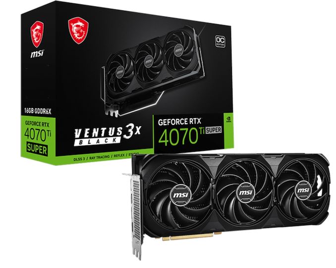
As GPU families enter the later part of their lifecycles, we often see chip manufacturers start to offload stockpiles of salvaged chips that, for one reason or another, didn't make the grade for the tier of cards they normally are used in. These recovered chips are fairly unremarkable overall, but they are unsold silicon that still works and has economic value, leading to them being used in lower-tier cards so that they can be sold. And, judging by the appearance of a new video card design from MSI, it looks like NVIDIA's Ada Lovelace generation of chips has reached that stage, as the Taiwanese video card maker has put out a new GeForce RTX 4070 Ti Super card based on a salvaged AD102 GPU.
Typically based on NVIDIA's AD103 GPU, NVIDIA's GeForce RTX 4070 Ti Super series sits a step below the company's flagship RTX 4080/4090 cards, both of which are based on the bigger and badder AD102 chip. But with some number of AD102 chips inevitably failing to live up to RTX 4080 specifications, rather than being thrown out, these chips can instead be used to make RTX 4070 cards. Which is exactly what MSI has done with their new GeForce RTX 4070 Ti Super Ventus 3X Black OC graphics card.
The card itself is relatively unremarkable – using a binned AD102 chip doesn't come with any advantages, and it should perform just like regular AD103 cards – and for that reason, video card vendors rarely publicly note when they're doing a run of cards with a binned-down version of a bigger chip. However, these larger chips have a tell-tale PCB footprint that usually makes it obvious what's going on. Which, as first noticed by @wxnod, is exactly what's going on with MSI's card.
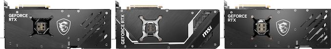
Ada Lovelace Lineup: MSI GeForce RTX 4070 TiS (AD103), RTX 4070 TiS (AD102), & RTX 4090 (AD102)
The tell, in this case, is the rear board shot provided by MSI. The larger AD102 GPU uses an equally larger mounting bracket, and is paired with a slightly more complex array of filtering capacitors on the back side of the board PCB. Ultimately, since these are visible in MSI's photos of their GeForce RTX 4070 Ti Super Ventus 3X Black OC, it's easy to compare it to other video cards and see that it has exactly the same capacitor layout as MSI's GeForce RTX 4090, thus confirming the use of an AD102 GPU.
Chip curiosities aside, all of NVIDIA GeForce RTX 4070 Ti Super graphics cards – no matter whether they are based on the AD102 or AD103 GPU – come with a GPU with 8,448 active CUDA cores and 16 GB of GDDR6X memory, so it doesn't (typically) matter which chip they carry. Otherwise, compared to a fully-enabled AD102 chip, the RTX 4070 Ti Super specifications are relatively modest, with fewer than half as many CUDA cores, underscoring how the AD102 chip being used in MSI's card is a pretty heavy salvage bin.
As for the rest of the card, MSI GeForce RTX 4070 Ti Super Ventus 3X Black OC is a relatively hefty card overall, with a cooling system to match. Being overclocked, the Ventus also has a slightly higher TDP than normal GeForce RTX 4070 Ti Super cards, weighing in at 295 Watts, or 10 Watts above baseline cards.
Meanwhile, MSI is apparently not the only video card manufacturer using salvaged AD102 chips for GeForce RTX 4070 Ti Super, either. @wxnod has also posted a screenshot obtained on an Inno3D GeForce RTX 4070 Ti Super based on an AD102 GPU.
GPUs
As GPU families enter the later part of their lifecycles, we often see chip manufacturers start to offload stockpiles of salvaged chips that, for one reason or another, didn't make the grade for the tier of cards they normally are used in. These recovered chips are fairly unremarkable overall, but they are unsold silicon that still works and has economic value, leading to them being used in lower-tier cards so that they can be sold. And, judging by the appearance of a new video card design from MSI, it looks like NVIDIA's Ada Lovelace generation of chips has reached that stage, as the Taiwanese video card maker has put out a new GeForce RTX 4070 Ti Super card based on a salvaged AD102 GPU.
Typically based on NVIDIA's AD103 GPU, NVIDIA's GeForce RTX 4070 Ti Super series sits a step below the company's flagship RTX 4080/4090 cards, both of which are based on the bigger and badder AD102 chip. But with some number of AD102 chips inevitably failing to live up to RTX 4080 specifications, rather than being thrown out, these chips can instead be used to make RTX 4070 cards. Which is exactly what MSI has done with their new GeForce RTX 4070 Ti Super Ventus 3X Black OC graphics card.
The card itself is relatively unremarkable – using a binned AD102 chip doesn't come with any advantages, and it should perform just like regular AD103 cards – and for that reason, video card vendors rarely publicly note when they're doing a run of cards with a binned-down version of a bigger chip. However, these larger chips have a tell-tale PCB footprint that usually makes it obvious what's going on. Which, as first noticed by @wxnod, is exactly what's going on with MSI's card.
Ada Lovelace Lineup: MSI GeForce RTX 4070 TiS (AD103), RTX 4070 TiS (AD102), & RTX 4090 (AD102)
The tell, in this case, is the rear board shot provided by MSI. The larger AD102 GPU uses an equally larger mounting bracket, and is paired with a slightly more complex array of filtering capacitors on the back side of the board PCB. Ultimately, since these are visible in MSI's photos of their GeForce RTX 4070 Ti Super Ventus 3X Black OC, it's easy to compare it to other video cards and see that it has exactly the same capacitor layout as MSI's GeForce RTX 4090, thus confirming the use of an AD102 GPU.
Chip curiosities aside, all of NVIDIA GeForce RTX 4070 Ti Super graphics cards – no matter whether they are based on the AD102 or AD103 GPU – come with a GPU with 8,448 active CUDA cores and 16 GB of GDDR6X memory, so it doesn't (typically) matter which chip they carry. Otherwise, compared to a fully-enabled AD102 chip, the RTX 4070 Ti Super specifications are relatively modest, with fewer than half as many CUDA cores, underscoring how the AD102 chip being used in MSI's card is a pretty heavy salvage bin.
As for the rest of the card, MSI GeForce RTX 4070 Ti Super Ventus 3X Black OC is a relatively hefty card overall, with a cooling system to match. Being overclocked, the Ventus also has a slightly higher TDP than normal GeForce RTX 4070 Ti Super cards, weighing in at 295 Watts, or 10 Watts above baseline cards.
Meanwhile, MSI is apparently not the only video card manufacturer using salvaged AD102 chips for GeForce RTX 4070 Ti Super, either. @wxnod has also posted a screenshot obtained on an Inno3D GeForce RTX 4070 Ti Super based on an AD102 GPU.
GPUs
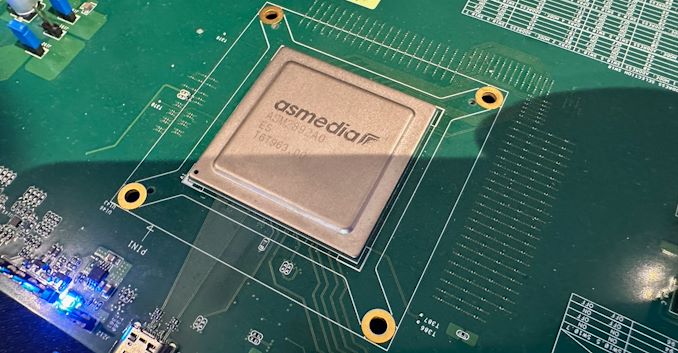
The USB Implementers Forum (USB-IF) introduced USB4 version 2.0 in fall 2022, and it expects systems and devices with the tech to emerge later this year and into next year. These upcoming products will largely rely on Intel's Barlow Ridge controller, a full-featured Thunderbolt 5 controller that goes above and beond the baseline USB4 v2 spec. And though extremely capable, Intel's Thunderbolt controllers are also quite expensive, and Barlow Ridge isn't expected to be any different. Fortunately, for system and device vendors that just need a basic USB4 v2 solution, ASMedia is also working on its own USB4 v2 controller.
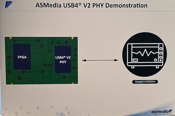
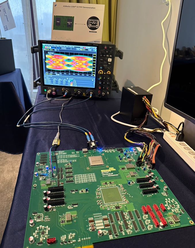
At Computex 2024, ASMedia demonstrated a prototype of its upcoming USB4 v2 physical interface (PHY), which will support USB4 v2's new Gen 4 (160Gbps) data rates and the associated PAM-3 signal encoding. The prototype was implemented using an FPGA, as the company yet has to tape out the completed controller.
Ultimately, the purpose of showing off a FPGA-based PHY at Computex was to allow ASMedia to demonstrate their current PHY design. With the shift to PAM-3 encoding for USB4 v2, ASMedia (and the rest of the USB ecosystem) must develop significantly more complex controllers – and there's no part of that more critical than a solid and reliable PHY design.
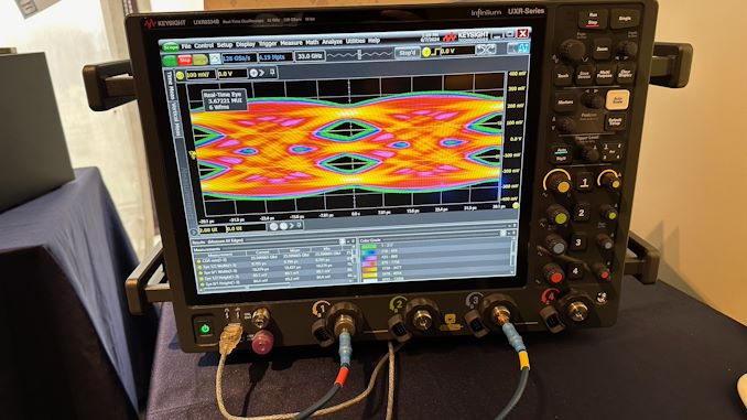
As part of their demonstration, ASMedia had a classic eye diagram display. The eye diagram demoed has a clear opening in the center, which is indicative of good signal integrity, as the larger the eye opening, the less distortion and noise in the signal. The horizontal width of the eye opening represents the time window in which the signal can be sampled correctly, so the relatively narrow horizontal spread of the eye opening suggests that there is minimal jitter, meaning the signal transitions are consistent and predictable. Finally, the vertical height of the eye opening indicates the signal amplitude and the rather tall eye opening suggests a higher signal-to-noise ratio (SNR), meaning that the signal is strong compared to any noise present.
ASMedia itself is one of the major suppliers for discrete USB controllers, so the availability of ASMedia's USB4 v2 chip is crucial for adoption of the standard in general. While Intel will spearhead the industry with their Barlow Ridge Thunderbolt 5/USB4 v2 controller, ASMedia's controller is poised to end up in a far larger range of devices. So the importance of the company's USB4 v2 PHY demo is hard to overstate.
Demos aside, ASMedia is hoping to tape the chip out soon. If all goes well, the company expects their first USB4 v2 controllers to hit the market some time in the second half of 2025.

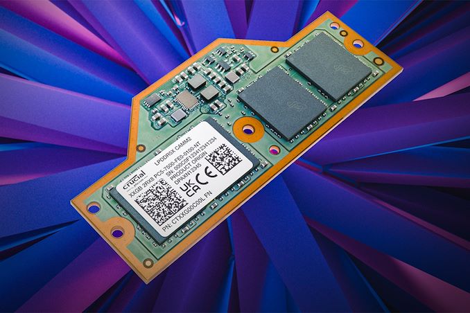
As LPCAMM2 adoption begins, the first retail memory modules are finally starting to hit the retail market, courtesy of Micron. The memory manufacturer has begun selling their LPDDR5X-based LPCAMM2 memory modules under their in-house Crucial brand, making them available on the latter's storefront. Timed to coincide with the release of Lenovo's ThinkPad P1 Gen 7 laptop – the first retail laptop designed to use the memory modules – this marks the de facto start of the eagerly-awaited modular LPDDR5X memory era.
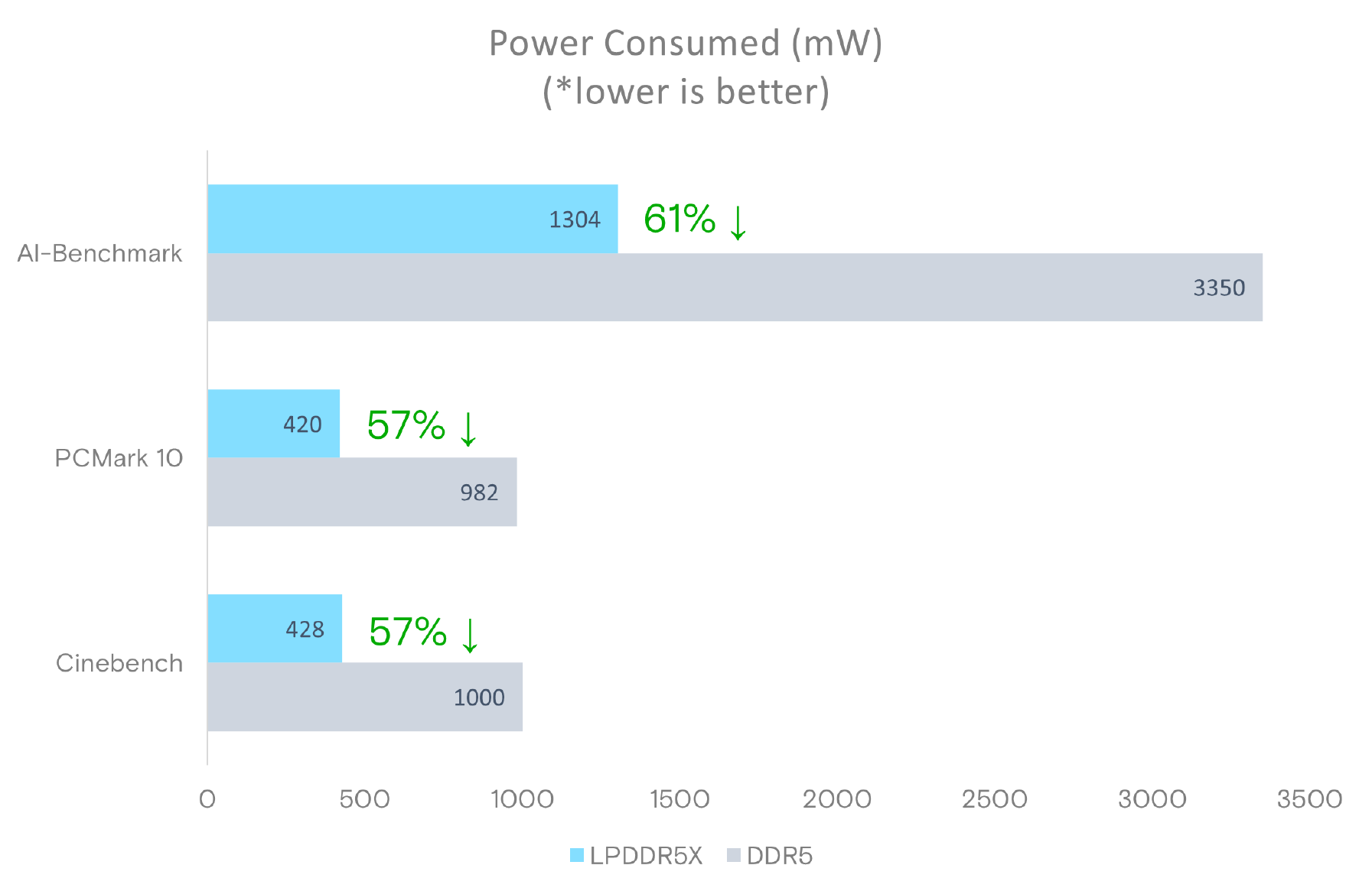
Micron's Low Power Compression Attached Memory Module 2 (LPCAMM2) modules are available in capacities of 32 GB and 64 GB. These are dual-channel modules that feature a 128-bit wide interface, and are based around LPDDR5X memory running at data rates up to 7500 MT/s. This gives a single LPCAMM2 a peak bandwidth of 120 GB/s. Micron is not disclosing the latencies of its LPCAMM2 memory modules, but it says that high data transfer rates of LPDDR5X compensate for the extended timings.
Micron says that LPDDR5X memory offers significantly lower power consumption, with active power per 64-bit bus being 43-58% lower than DDR5 at the same speed, and standby power up to 80% lower. Meanwhile, similar to DDR5 modules, LPCAMM2 modules include a power management IC and voltage regulating circuitry, which provides module manufacturers additional opportunities to reduce power consumption of their products.
Source: Micron LPDDR5X LPCAMM2 Technical Brief
It's worth noting, however, that at least for the first generation of LPCAMM2 modules, system vendors will need to pick between modularity and performance. While soldered-down LPDDR5X memory is available at speeds up to 8533 MT/sec – and with 9600 MT/sec on the horizon – the fastest LPCAMM2 modules planned for this year by both Micron and rival Samsung will be running at 7500 MT/sec. So vendors will have to choose between the flexibility of offering modular LPDDR5X, or the higher bandwidth (and space savings) offered by soldering down their memory.
Micron, for its part, is projecting that 9600 MT/sec LPCAMM2 modules will be available by 2026. Though it's all but certain that faster memory will also be avaialble in the same timeframe.
Micron's Crucial LPDDR5X 32 GB module costs $174.99, whereas a 64 GB module costs $329.99.
Memory
Lorem Ipsum is simply dummy text of the printing and typesetting industry. Lorem Ipsum has been the industry's.


 for its AI initiatives, and then <a href="https://www.tomshardware.com/news/intel-replaces-xeons-with-custom-vcus">video transcoding units (VCUs)</a> for the YouTube service. But unlike its industry peers, the company has been slower to adopt custom CPU designs, prefering to stick to off-the-shelf chips from the major CPUs. This is finally changing at Google, with the announcement that the company has developed its own in-house datacenter CPU, the Axion.</p>
<p>Google's Axion processor is based on the <a href="https://www.anandtech.com/show/17575/arm-announces-neoverse-v2-and-e2-the-next-generation-of-arm-server-cpu-cores">Arm Neoverse V2</a> (Arm v9) platform, which is Arm's current-generation design for high-performance server CPUs, and is already employed in other chips such as NVIDIA's Grace and Amazon's Graviton4. Within Google, Axion is aimed at a wide variety of workloads, including web and app servers, data analytics, microservices, and AI training. Google claims that the Axion processors boast up to 50% higher performance and up to 60% better energy efficiency compared to current-generation x86-based processors, as well as offer a 30% higher performance compared to competing Arm-based CPUs for datacenters. Though as is increasingly common for the cryptic cloud side of Google's business, least for now the company isn't specifying what processors they're comparing Axion to in these metrics.</p>
<p>While Google is not disclosing core counts or the full specifications of its Axion CPUs, the company is revealing that they are incorporating their own secret sauce into the silicon in the form of the company's <a href="https://cloud.google.com/titanium?e=48754805&hl=en">Titanium</a> purpose-built microcontrollers. These microcontrollers are designed to handle basic operations like networking and security, as well as offload storage I/O processing to Hyperdisk block storage service. As a result of this offloading, virtually all of the CPU core resources should be available to actual workloads. As for the chip's memory subsystem, Axion uses conventional dual-rank DDR5 memory modules.</p>
<p>"Google's announcement of the new Axion CPU marks a significant milestone in delivering custom silicon that is optimized for Google's infrastructure, and built on our high-performance Arm Neoverse V2 platform," said Rene Haas, CEO of Arm. "Decades of ecosystem investment, combined with Google's ongoing innovation and open-source software contributions ensure the best experience for the workloads that matter most to customers running on Arm everywhere." </p>
<p>Google has previously deployed Arm-based processors for its own services, including BigTable, Spanner, BigQuery, and YouTube Ads and is ready to offer instances based on its Armv9-based Axion CPUs to its customers that can use software developed for Arm architectures.</p>
<p>Sources: <a href="https://cloud.google.com/blog/products/compute/introducing-googles-new-arm-based-cpu">Google</a>, <a href="https://www.wsj.com/tech/google-expands-in-house-chip-efforts-in-costly-ai-battle-3121c852?st=6010gt7v4bee9ve&reflink=desktopwebshare_permalink&s=31">Wall Street Journal</a></p>
</p> CPUs)
 for its AI initiatives, and then <a href="https://www.tomshardware.com/news/intel-replaces-xeons-with-custom-vcus">video transcoding units (VCUs)</a> for the YouTube service. But unlike its industry peers, the company has been slower to adopt custom CPU designs, prefering to stick to off-the-shelf chips from the major CPUs. This is finally changing at Google, with the announcement that the company has developed its own in-house datacenter CPU, the Axion.</p>
<p>Google's Axion processor is based on the <a href="https://www.anandtech.com/show/17575/arm-announces-neoverse-v2-and-e2-the-next-generation-of-arm-server-cpu-cores">Arm Neoverse V2</a> (Arm v9) platform, which is Arm's current-generation design for high-performance server CPUs, and is already employed in other chips such as NVIDIA's Grace and Amazon's Graviton4. Within Google, Axion is aimed at a wide variety of workloads, including web and app servers, data analytics, microservices, and AI training. Google claims that the Axion processors boast up to 50% higher performance and up to 60% better energy efficiency compared to current-generation x86-based processors, as well as offer a 30% higher performance compared to competing Arm-based CPUs for datacenters. Though as is increasingly common for the cryptic cloud side of Google's business, least for now the company isn't specifying what processors they're comparing Axion to in these metrics.</p>
<p>While Google is not disclosing core counts or the full specifications of its Axion CPUs, the company is revealing that they are incorporating their own secret sauce into the silicon in the form of the company's <a href="https://cloud.google.com/titanium?e=48754805&hl=en">Titanium</a> purpose-built microcontrollers. These microcontrollers are designed to handle basic operations like networking and security, as well as offload storage I/O processing to Hyperdisk block storage service. As a result of this offloading, virtually all of the CPU core resources should be available to actual workloads. As for the chip's memory subsystem, Axion uses conventional dual-rank DDR5 memory modules.</p>
<p>"Google's announcement of the new Axion CPU marks a significant milestone in delivering custom silicon that is optimized for Google's infrastructure, and built on our high-performance Arm Neoverse V2 platform," said Rene Haas, CEO of Arm. "Decades of ecosystem investment, combined with Google's ongoing innovation and open-source software contributions ensure the best experience for the workloads that matter most to customers running on Arm everywhere." </p>
<p>Google has previously deployed Arm-based processors for its own services, including BigTable, Spanner, BigQuery, and YouTube Ads and is ready to offer instances based on its Armv9-based Axion CPUs to its customers that can use software developed for Arm architectures.</p>
<p>Sources: <a href="https://cloud.google.com/blog/products/compute/introducing-googles-new-arm-based-cpu">Google</a>, <a href="https://www.wsj.com/tech/google-expands-in-house-chip-efforts-in-costly-ai-battle-3121c852?st=6010gt7v4bee9ve&reflink=desktopwebshare_permalink&s=31">Wall Street Journal</a></p>
</p> CPUs | https://compbuddey.blogspot.com/2024/04/google-develops-in-house-arm-axion-cpu_20.html)
 for its AI initiatives, and then <a href="https://www.tomshardware.com/news/intel-replaces-xeons-with-custom-vcus">video transcoding units (VCUs)</a> for the YouTube service. But unlike its industry peers, the company has been slower to adopt custom CPU designs, prefering to stick to off-the-shelf chips from the major CPUs. This is finally changing at Google, with the announcement that the company has developed its own in-house datacenter CPU, the Axion.</p>
<p>Google's Axion processor is based on the <a href="https://www.anandtech.com/show/17575/arm-announces-neoverse-v2-and-e2-the-next-generation-of-arm-server-cpu-cores">Arm Neoverse V2</a> (Arm v9) platform, which is Arm's current-generation design for high-performance server CPUs, and is already employed in other chips such as NVIDIA's Grace and Amazon's Graviton4. Within Google, Axion is aimed at a wide variety of workloads, including web and app servers, data analytics, microservices, and AI training. Google claims that the Axion processors boast up to 50% higher performance and up to 60% better energy efficiency compared to current-generation x86-based processors, as well as offer a 30% higher performance compared to competing Arm-based CPUs for datacenters. Though as is increasingly common for the cryptic cloud side of Google's business, least for now the company isn't specifying what processors they're comparing Axion to in these metrics.</p>
<p>While Google is not disclosing core counts or the full specifications of its Axion CPUs, the company is revealing that they are incorporating their own secret sauce into the silicon in the form of the company's <a href="https://cloud.google.com/titanium?e=48754805&hl=en">Titanium</a> purpose-built microcontrollers. These microcontrollers are designed to handle basic operations like networking and security, as well as offload storage I/O processing to Hyperdisk block storage service. As a result of this offloading, virtually all of the CPU core resources should be available to actual workloads. As for the chip's memory subsystem, Axion uses conventional dual-rank DDR5 memory modules.</p>
<p>"Google's announcement of the new Axion CPU marks a significant milestone in delivering custom silicon that is optimized for Google's infrastructure, and built on our high-performance Arm Neoverse V2 platform," said Rene Haas, CEO of Arm. "Decades of ecosystem investment, combined with Google's ongoing innovation and open-source software contributions ensure the best experience for the workloads that matter most to customers running on Arm everywhere." </p>
<p>Google has previously deployed Arm-based processors for its own services, including BigTable, Spanner, BigQuery, and YouTube Ads and is ready to offer instances based on its Armv9-based Axion CPUs to its customers that can use software developed for Arm architectures.</p>
<p>Sources: <a href="https://cloud.google.com/blog/products/compute/introducing-googles-new-arm-based-cpu">Google</a>, <a href="https://www.wsj.com/tech/google-expands-in-house-chip-efforts-in-costly-ai-battle-3121c852?st=6010gt7v4bee9ve&reflink=desktopwebshare_permalink&s=31">Wall Street Journal</a></p>
</p> CPUs&body=https://compbuddey.blogspot.com/2024/04/google-develops-in-house-arm-axion-cpu_20.html)
0 Comments