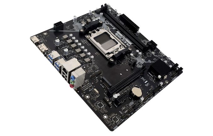

BIOSTAR has launched its AM5-based A620MS motherboard today, bringing a new low-end option for PC users on a budget. Though BIOSTAR has not disclosed what MSRP it the A620MS motherboard will carry, the specifications of the board make it clear that it targets the lowest-end segment of the market, though it makes use of the regular A620 chipset instead of the even less expensive A620A chipset.
The A620MS sports some features typical for mATX A620 boards (which make up the vast majority of current models): two DDR5 DIMM slots that support up to two 48GB sticks, an M.2 PCIe 4.0 slot for SSDs, four SATA III ports, and a PCIe Gen4 x16 slot. The motherboard also has four debug LEDs for diagnosing CPU, RAM, GPU, and booting errors.
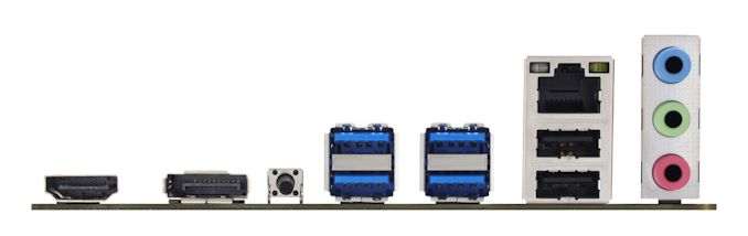
Meanwhile the rear I/O features a one gigabit Ethernet port, four USB 3.2 ports, analog audio jacks, two USB 2.0 ports, an HDMI 1.4 port, and DisplayPort 1.2. Though there are some more fully-featured A620 motherboards available with more ports operating at a higher specification, but the rear I/O is more or less par for the course when it comes to A620.
However, there are other things about BIOSTAR’s A620MS that implies it will be quite low-end for an A620 motherboard. It has just eight total voltage regulator modules (VRMs), which appear to be in a 6+2 or 6+1+1 phase configuration. This isn’t as low-end as BIOSTAR could have gone (ASRock offers a 4+1+1 stage board), but it is still very sparing in VRM stages compared to most other A620 motherboards. These VRMs are also not covered by a heatsink, which is also typical for boards in this segment, as they're normally paired with equally chip 65W(ish) chips.
BIOSTAR doesn’t list any official CPU restrictions in either its press release or its specification sheet; instead, the company simply lists the motherboard as compatible with Ryzen 7000 and future Ryzen 8000 processors.
While the market for AM5 motherboards includes plenty of B650(E) and X670(E) models, there’s only a handful of A620 boards in total. On Newegg, there are 14 different motherboards available, and many only differ slightly in respect to things like form factor. The cheapest of these cost $75 to $100, and while BIOSTAR didn’t reveal what price we should expect of its A620MS board, given its specifications, we expect it will land in that same $75 to $100 region.
Motherboards

Demand for high-performance processors for AI training is skyrocketing, and consequently so is the demand for the components that go into these processors. So much so that SK hynix this week is very publicly announcing that the company's high-bandwidth memory (HBM) production capacity has already sold out for the rest of 2024, and even most of 2025 has already sold out as well.
SK hynix currently produces various types of HBM memory for customers like Amazon, AMD, Facebook, Google (Broadcom), Intel, Microsoft, and, of course, NVIDIA. The latter is an especially prolific consumer of HBM3 and HBM3E memory for its H100/H200/GH200 accelerators, as NVIDIA is also working to fill what remains an insatiable (and unmet) demand for its accelerators.
As a result, HBM memory orders, which are already placed months in advance, are now backlogging well into 2025 as chip vendors look to secure supplies of the memory stacks critical to their success.
This has made SK hynix the secnd HBM memory vendor in recent months to announce that they've sold out into 2025, following an earlier announcement from Micron regarding its HBM3E production. But of the two announcements, SK hynix's is arguably the most significant yet, as the South Korean firm's HBM production capacity is far greater than Micron's. So while things were merely "interesting" with the smallest of the Big Three memory manufacturers being sold out into 2025, things are taking a more concerning (and constrained) outlook now that SK hynix is as well.
SK hynix currently controls roughly 46% - 49% of HBM market, and its share is not expected to drop significantly in 2025, according to market tracking firm TrendForce. By contrast, Micron's share on HBM memory market is between 4% and 6%. Since HBM supply of both companies is sold out through the most of 2025, we're likely looking at a scenario where over 50% of the industry's total HBM3/HBM3E supply for the coming quarters is already sold out.
This leaves Samsung as the only member of the group not to comment on HBM demand so far. Though with memory being a highly fungible commodity product, it would be surprising if Samsung wasn't facing similar demand. And, ultimately, all of this is pointing towards the indusry entering an HBM3 memory shortage.
Separately, SK hynix said that it is sampling 12-Hi 36GB HBM3E stacks with customers and will begin volume shipments in the third quarter.
Memory![Micron: U.S. Fabs Will Start Operating in 2026 - 2029 <p align="center"><a href="https://www.anandtech.com/show/21459/micron-u-s-fabs-will-start-operating-in-2026-2029"><img src="https://images.anandtech.com/doci/21459/micron-server-datacenter-general-generic-678_575px.jpg" alt="" /></a></p><p><p>When Micron announced plans to build two new fabs in the U.S. in 2022, the company vaguely said both would come online by the decade's end. Then, in 2023, it began to optimize its spending, which pushed production at these fabrication facilities. This week, the company outlined more precise timeframes for when its fabs in <a href="https://www.anandtech.com/show/17573/micron-breaks-ground-on-its-15-billion-euv-dram-fab-in-the-us">Idaho</a> and <a href="https://www.anandtech.com/show/17606/micron-announces-100-billion-us-fab-complex-a-20year-plan">New York</a> will start operations: this will happen from calendar 2026 to calendar 2029.</p>
<p>"<em>These fab construction investments are necessary to support supply growth for the latter half of this decade,</em>" a statement by Micron in its Q3 FY2024 financial results report <a href="https://investors.micron.com/static-files/a531c7f0-fca2-48f3-8f24-79c945aaa2d2">reads</a>. "<em>This Idaho fab will not contribute to meaningful bit supply until fiscal 2027 and the New York construction capex is not expected to contribute to bit supply growth until fiscal 2028 or later. The timing of future [wafer fab equipment] spend in these fabs will be managed to align supply growth with expected demand growth.</em>"</p>
<p>Micron's fiscal year 2027 starts in September 2026, so the new fab near Boise, Idaho, is set to start operations between September 2026 and September 2027. The company's fiscal 2028 starts in September 2027, so the fab will likely begin operations in calendar 2028 or later, probably depending on the demand for DRAM memory in the coming years. That said, Micron's U.S. memory fabs will begin operations between late 2026 and 2029, which aligns with the company's original plans. </p>
<p>Construction of the fab in Idaho is well underway. In contrast, construction of the New York facility has yet to begin as the company is working on regulatory and permitting processes in the state. </p>
<p>Micron's capital expenditure (CaPex) plan for FY2024 is approximately $8.0 billion, with a decrease in year-over-year spending on wafer fabrication equipment (WFE). In Q4 FY2024, the company will spend around $3 billion on fab construction, new wafer fab tools, and various expansions/upgrades.</p>
<p>Looking ahead to FY2025, the company plans a substantial increase in capex, targeting a mid-30s percentage of revenue to support various technological and facility advancements. In particular, it expects its quarterly CapEx to average above the $3 billion level seen in the fourth quarter of FY2024, which means that it plans to spend about $12 billion in its fiscal 2025, which begins in late September.</p>
<p>Half or more of the total CapEx increase in FY2025 (i.e., over $2 billion) will be allocated to constructing new fabs in Idaho and New York. Meanwhile, the FY2025 CapEx will significantly rise to fund high-bandwidth memory (HBM) assembly and testing and the construction of fabrication and back-end facilities. This increase also includes investments in technology transitions to meet growing demand. </p>
<p>"<em>Fab construction in Idaho is underway, and we are working diligently to complete the regulatory and permitting processes in New York,</em>" said Sanjay Mehrotra, chief executive officer of Micron, at the company's conference call with investors and financial analysts (via <a href="https://seekingalpha.com/article/4701253-micron-technology-inc-mu-q3-2024-earnings-call-transcript?source=content_type%3Areact%7Csection%3ATranscripts%7Csection_asset%3ATranscripts%7Cfirst_level_url%3Asymbol%7Cbutton%3ATitle%7Clock_status%3ANo%7Cline%3A1">SeekingAlpha</a>). "<em>This additional leading-edge greenfield capacity, along with continued technology transition investments in our Asia facilities, is required to meet long-term demand in the second half of this decade and beyond. These investments support our objective to maintain our current bit share over time and to grow our memory bit supply in line with long-term industry bit demand.</em>"</p>
</p> Memory](https://lh3.googleusercontent.com/blogger_img_proxy/AEn0k_tcBPi9WX2hkRsEO9qWM_vX3xGKwpZixKDt-L7q2x_bPLeaj4YZ6_w19D4xNh3uPh2IcFfewutmeNfEEWS6Z5JZecWBtVbWgbb7c75w5GoCWRlOl_WeEaDPpsr6xITMoT2Bwi-n1iEgfK-HSrLCft30zOn8F5012934P3bU4-zi1Vg=w72-h72-p-k-no-nu)

When Micron announced plans to build two new fabs in the U.S. in 2022, the company vaguely said both would come online by the decade's end. Then, in 2023, it began to optimize its spending, which pushed production at these fabrication facilities. This week, the company outlined more precise timeframes for when its fabs in Idaho and New York will start operations: this will happen from calendar 2026 to calendar 2029.
"These fab construction investments are necessary to support supply growth for the latter half of this decade," a statement by Micron in its Q3 FY2024 financial results report reads. "This Idaho fab will not contribute to meaningful bit supply until fiscal 2027 and the New York construction capex is not expected to contribute to bit supply growth until fiscal 2028 or later. The timing of future [wafer fab equipment] spend in these fabs will be managed to align supply growth with expected demand growth."
Micron's fiscal year 2027 starts in September 2026, so the new fab near Boise, Idaho, is set to start operations between September 2026 and September 2027. The company's fiscal 2028 starts in September 2027, so the fab will likely begin operations in calendar 2028 or later, probably depending on the demand for DRAM memory in the coming years. That said, Micron's U.S. memory fabs will begin operations between late 2026 and 2029, which aligns with the company's original plans.
Construction of the fab in Idaho is well underway. In contrast, construction of the New York facility has yet to begin as the company is working on regulatory and permitting processes in the state.
Micron's capital expenditure (CaPex) plan for FY2024 is approximately $8.0 billion, with a decrease in year-over-year spending on wafer fabrication equipment (WFE). In Q4 FY2024, the company will spend around $3 billion on fab construction, new wafer fab tools, and various expansions/upgrades.
Looking ahead to FY2025, the company plans a substantial increase in capex, targeting a mid-30s percentage of revenue to support various technological and facility advancements. In particular, it expects its quarterly CapEx to average above the $3 billion level seen in the fourth quarter of FY2024, which means that it plans to spend about $12 billion in its fiscal 2025, which begins in late September.
Half or more of the total CapEx increase in FY2025 (i.e., over $2 billion) will be allocated to constructing new fabs in Idaho and New York. Meanwhile, the FY2025 CapEx will significantly rise to fund high-bandwidth memory (HBM) assembly and testing and the construction of fabrication and back-end facilities. This increase also includes investments in technology transitions to meet growing demand.
"Fab construction in Idaho is underway, and we are working diligently to complete the regulatory and permitting processes in New York," said Sanjay Mehrotra, chief executive officer of Micron, at the company's conference call with investors and financial analysts (via SeekingAlpha). "This additional leading-edge greenfield capacity, along with continued technology transition investments in our Asia facilities, is required to meet long-term demand in the second half of this decade and beyond. These investments support our objective to maintain our current bit share over time and to grow our memory bit supply in line with long-term industry bit demand."
Memory

Kioxia's booth at FMS 2024 was a busy one with multiple technology demonstrations keeping visitors occupied. A walk-through of the BiCS 8 manufacturing process was the first to grab my attention. Kioxia and Western Digital announced the sampling of BiCS 8 in March 2023. We had touched briefly upon its CMOS Bonded Array (CBA) scheme in our coverage of Kioxial's 2Tb QLC NAND device and coverage of Western Digital's 128 TB QLC enterprise SSD proof-of-concept demonstration. At Kioxia's booth, we got more insights.

Traditionally, fabrication of flash chips involved placement of the associate logic circuitry (CMOS process) around the periphery of the flash array. The process then moved on to putting the CMOS under the cell array, but the wafer development process was serialized with the CMOS logic getting fabricated first followed by the cell array on top. However, this has some challenges because the cell array requires a high-temperature processing step to ensure higher reliability that can be detrimental to the health of the CMOS logic. Thanks to recent advancements in wafer bonding techniques, the new CBA process allows the CMOS wafer and cell array wafer to be processed independently in parallel and then pieced together, as shown in the models above.

The BiCS 8 3D NAND incorporates 218 layers, compared to 112 layers in BiCS 5 and 162 layers in BiCS 6. The company decided to skip over BiCS 7 (or, rather, it was probably a short-lived generation meant as an internal test vehicle). The generation retains the four-plane charge trap structure of BiCS 6. In its TLC avatar, it is available as a 1 Tbit device. The QLC version is available in two capacities - 1 Tbit and 2 Tbit.
Kioxia also noted that while the number of layers (218) doesn't compare favorably with the latest layer counts from the competition, its lateral scaling / cell shrinkage has enabled it to be competitive in terms of bit density as well as operating speeds (3200 MT/s). For reference, the latest shipping NAND from Micron - the G9 - has 276 layers with a bit density in TLC mode of 21 Gbit/mm2, and operates at up to 3600 MT/s. However, its 232L NAND operates only up to 2400 MT/s and has a bit density of 14.6 Gbit/mm2.
It must be noted that the CBA hybrid bonding process has advantages over the current processes used by other vendors - including Micron's CMOS under array (CuA) and SK hynix's 4D PUC (periphery-under-chip) developed in the late 2010s. It is expected that other NAND vendors will also move eventually to some variant of the hybrid bonding scheme used by Kioxia.
Storage
Lorem Ipsum is simply dummy text of the printing and typesetting industry. Lorem Ipsum has been the industry's.


: two DDR5 DIMM slots that support up to two 48GB sticks, an M.2 PCIe 4.0 slot for SSDs, four SATA III ports, and a PCIe Gen4 x16 slot. The motherboard also has four debug LEDs for diagnosing CPU, RAM, GPU, and booting errors.</p>
<p>Meanwhile the rear I/O features a one gigabit Ethernet port, four USB 3.2 ports, analog audio jacks, two USB 2.0 ports, an HDMI 1.4 port, and DisplayPort 1.2. Though there are some more fully-featured A620 motherboards available with more ports operating at a higher specification, but the rear I/O is more or less par for the course when it comes to A620.</p>
<p align="center"><a href="https://www.anandtech.com/show/21305/biostar-debuts-barebones-a620ms-matx-motherboard-for-ryzen-7000-processors"><img alt="" src="https://images.anandtech.com/doci/21305/BIOSTAR-A620S-IO_575px.jpg" /></a></p>
<p>However, there are other things about BIOSTAR’s A620MS that implies it will be quite low-end for an A620 motherboard. It has just eight total voltage regulator modules (VRMs), which appear to be in a 6+2 or 6+1+1 phase configuration. This isn’t as low-end as BIOSTAR could have gone (ASRock offers a 4+1+1 stage board), but it is still very sparing in VRM stages compared to most other A620 motherboards. These VRMs are also not covered by a heatsink, which is also typical for boards in this segment, as they're normally paired with equally chip 65W(ish) chips.</p>
<p>BIOSTAR doesn’t list any official CPU restrictions in either its press release or its specification sheet; instead, the company simply lists the motherboard as compatible with Ryzen 7000 and future Ryzen 8000 processors.</p>
<p>While the market for AM5 motherboards includes plenty of B650(E) and X670(E) models, there’s only a handful of A620 boards in total. On <a href="https://click.linksynergy.com/deeplink?id=kXQk6%2AivFEQ&mid=44583&u1=anandtech-us-6136182386955096263&murl=https%3A%2F%2Fwww.newegg.com%2Fp%2Fpl%3FN%3D100007625%2520601414319%25208000%26Order%3D1">Newegg</a>, there are 14 different motherboards available, and many only differ slightly in respect to things like form factor. The cheapest of these cost $75 to $100, and while BIOSTAR didn’t reveal what price we should expect of its A620MS board, given its specifications, we expect it will land in that same $75 to $100 region.</p>
</p> Motherboards)
: two DDR5 DIMM slots that support up to two 48GB sticks, an M.2 PCIe 4.0 slot for SSDs, four SATA III ports, and a PCIe Gen4 x16 slot. The motherboard also has four debug LEDs for diagnosing CPU, RAM, GPU, and booting errors.</p>
<p>Meanwhile the rear I/O features a one gigabit Ethernet port, four USB 3.2 ports, analog audio jacks, two USB 2.0 ports, an HDMI 1.4 port, and DisplayPort 1.2. Though there are some more fully-featured A620 motherboards available with more ports operating at a higher specification, but the rear I/O is more or less par for the course when it comes to A620.</p>
<p align="center"><a href="https://www.anandtech.com/show/21305/biostar-debuts-barebones-a620ms-matx-motherboard-for-ryzen-7000-processors"><img alt="" src="https://images.anandtech.com/doci/21305/BIOSTAR-A620S-IO_575px.jpg" /></a></p>
<p>However, there are other things about BIOSTAR’s A620MS that implies it will be quite low-end for an A620 motherboard. It has just eight total voltage regulator modules (VRMs), which appear to be in a 6+2 or 6+1+1 phase configuration. This isn’t as low-end as BIOSTAR could have gone (ASRock offers a 4+1+1 stage board), but it is still very sparing in VRM stages compared to most other A620 motherboards. These VRMs are also not covered by a heatsink, which is also typical for boards in this segment, as they're normally paired with equally chip 65W(ish) chips.</p>
<p>BIOSTAR doesn’t list any official CPU restrictions in either its press release or its specification sheet; instead, the company simply lists the motherboard as compatible with Ryzen 7000 and future Ryzen 8000 processors.</p>
<p>While the market for AM5 motherboards includes plenty of B650(E) and X670(E) models, there’s only a handful of A620 boards in total. On <a href="https://click.linksynergy.com/deeplink?id=kXQk6%2AivFEQ&mid=44583&u1=anandtech-us-6136182386955096263&murl=https%3A%2F%2Fwww.newegg.com%2Fp%2Fpl%3FN%3D100007625%2520601414319%25208000%26Order%3D1">Newegg</a>, there are 14 different motherboards available, and many only differ slightly in respect to things like form factor. The cheapest of these cost $75 to $100, and while BIOSTAR didn’t reveal what price we should expect of its A620MS board, given its specifications, we expect it will land in that same $75 to $100 region.</p>
</p> Motherboards | https://compbuddey.blogspot.com/2024/04/biostar-debuts-barebones-a620ms-matx_5.html)
: two DDR5 DIMM slots that support up to two 48GB sticks, an M.2 PCIe 4.0 slot for SSDs, four SATA III ports, and a PCIe Gen4 x16 slot. The motherboard also has four debug LEDs for diagnosing CPU, RAM, GPU, and booting errors.</p>
<p>Meanwhile the rear I/O features a one gigabit Ethernet port, four USB 3.2 ports, analog audio jacks, two USB 2.0 ports, an HDMI 1.4 port, and DisplayPort 1.2. Though there are some more fully-featured A620 motherboards available with more ports operating at a higher specification, but the rear I/O is more or less par for the course when it comes to A620.</p>
<p align="center"><a href="https://www.anandtech.com/show/21305/biostar-debuts-barebones-a620ms-matx-motherboard-for-ryzen-7000-processors"><img alt="" src="https://images.anandtech.com/doci/21305/BIOSTAR-A620S-IO_575px.jpg" /></a></p>
<p>However, there are other things about BIOSTAR’s A620MS that implies it will be quite low-end for an A620 motherboard. It has just eight total voltage regulator modules (VRMs), which appear to be in a 6+2 or 6+1+1 phase configuration. This isn’t as low-end as BIOSTAR could have gone (ASRock offers a 4+1+1 stage board), but it is still very sparing in VRM stages compared to most other A620 motherboards. These VRMs are also not covered by a heatsink, which is also typical for boards in this segment, as they're normally paired with equally chip 65W(ish) chips.</p>
<p>BIOSTAR doesn’t list any official CPU restrictions in either its press release or its specification sheet; instead, the company simply lists the motherboard as compatible with Ryzen 7000 and future Ryzen 8000 processors.</p>
<p>While the market for AM5 motherboards includes plenty of B650(E) and X670(E) models, there’s only a handful of A620 boards in total. On <a href="https://click.linksynergy.com/deeplink?id=kXQk6%2AivFEQ&mid=44583&u1=anandtech-us-6136182386955096263&murl=https%3A%2F%2Fwww.newegg.com%2Fp%2Fpl%3FN%3D100007625%2520601414319%25208000%26Order%3D1">Newegg</a>, there are 14 different motherboards available, and many only differ slightly in respect to things like form factor. The cheapest of these cost $75 to $100, and while BIOSTAR didn’t reveal what price we should expect of its A620MS board, given its specifications, we expect it will land in that same $75 to $100 region.</p>
</p> Motherboards&body=https://compbuddey.blogspot.com/2024/04/biostar-debuts-barebones-a620ms-matx_5.html)
0 Comments