


AMD's FidelityFX Super Resolution 3 technology package introduced a plethora of enhancements to the FSR technology on Radeon RX 6000 and 7000-series graphics cards last September. But perfection has no limits, so this week, the company is rolling out its FSR 3.1 technology, which improves upscaling quality, decouples frame generation from AMD's upscaling, and makes it easier for developers to work with FSR.
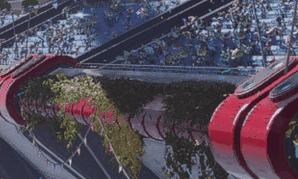
Arguably, AMD's FSR 3.1's primary enhancement is its improved temporal upscaling image quality: compared to FSR 2.2, the image flickers less at rest and no longer ghosts when in movement. This is a significant improvement, as flickering and ghosting artifacts are particularly annoying. Meanwhile, FSR 3.1 has to be implemented by the game developer itself, and the first title to support this new technology sometime later this year is Ratchet & Clank: Rift Apart.
| Temporal Stability | |
|
|
|
| AMD FSR 2.2 | AMD FSR 3.1 |
| Ghosting Reduction | |
|
|
|
| AMD FSR 2.2 | AMD FSR 3.1 |
Another significant development brought by FSR 3.1 is its decoupling from the Frame Generation feature introduced by FSR 3. This capability relies on a form of AMD's Fluid Motion Frames (AFMF) optical flow interpolation. It uses temporal game data like motion vectors to add an additional frame between existing ones. This ability can lead to a performance boost of up to two times in compatible games, but it was initially tied to FSR 3 upscaling, which is a limitation. Starting from FSR 3.1, it will work with other upscaling methods, though AMD refrains from saying which methods and on which hardware for now. Also, the company does not disclose when it is expected to be implemented by game developers.
In addition, AMD is bringing support for FSR3 to Vulkan and Xbox Game Development Kit, enabling game developers on these platforms to use it. It also adds FSR 3.1 to the FidelityFX API, which simplifies debugging and enables forward compatibility with updated versions of FSR.
Upon its release in September 2023, AMD FSR 3 was initially supported by two titles, Forspoken and Immortals of Aveum, with ten more games poised to join them back then. Fast forward to six months later, the lineup has expanded to an impressive roster of 40 games either currently supporting or set to incorporate FSR 3 shortly. As of March 2024, FSR is supported by games like Avatar: Frontiers of Pandora, Starfield, The Last of Us Part I. Shortly, Cyberpunk 2077, Dying Light 2 Stay Human, Frostpunk 2, and Ratchet & Clank: Rift Apart will support FSR shortly.
Source: AMD
GPUs![Micron: U.S. Fabs Will Start Operating in 2026 - 2029 <p align="center"><a href="https://www.anandtech.com/show/21459/micron-u-s-fabs-will-start-operating-in-2026-2029"><img src="https://images.anandtech.com/doci/21459/micron-server-datacenter-general-generic-678_575px.jpg" alt="" /></a></p><p><p>When Micron announced plans to build two new fabs in the U.S. in 2022, the company vaguely said both would come online by the decade's end. Then, in 2023, it began to optimize its spending, which pushed production at these fabrication facilities. This week, the company outlined more precise timeframes for when its fabs in <a href="https://www.anandtech.com/show/17573/micron-breaks-ground-on-its-15-billion-euv-dram-fab-in-the-us">Idaho</a> and <a href="https://www.anandtech.com/show/17606/micron-announces-100-billion-us-fab-complex-a-20year-plan">New York</a> will start operations: this will happen from calendar 2026 to calendar 2029.</p>
<p>"<em>These fab construction investments are necessary to support supply growth for the latter half of this decade,</em>" a statement by Micron in its Q3 FY2024 financial results report <a href="https://investors.micron.com/static-files/a531c7f0-fca2-48f3-8f24-79c945aaa2d2">reads</a>. "<em>This Idaho fab will not contribute to meaningful bit supply until fiscal 2027 and the New York construction capex is not expected to contribute to bit supply growth until fiscal 2028 or later. The timing of future [wafer fab equipment] spend in these fabs will be managed to align supply growth with expected demand growth.</em>"</p>
<p>Micron's fiscal year 2027 starts in September 2026, so the new fab near Boise, Idaho, is set to start operations between September 2026 and September 2027. The company's fiscal 2028 starts in September 2027, so the fab will likely begin operations in calendar 2028 or later, probably depending on the demand for DRAM memory in the coming years. That said, Micron's U.S. memory fabs will begin operations between late 2026 and 2029, which aligns with the company's original plans. </p>
<p>Construction of the fab in Idaho is well underway. In contrast, construction of the New York facility has yet to begin as the company is working on regulatory and permitting processes in the state. </p>
<p>Micron's capital expenditure (CaPex) plan for FY2024 is approximately $8.0 billion, with a decrease in year-over-year spending on wafer fabrication equipment (WFE). In Q4 FY2024, the company will spend around $3 billion on fab construction, new wafer fab tools, and various expansions/upgrades.</p>
<p>Looking ahead to FY2025, the company plans a substantial increase in capex, targeting a mid-30s percentage of revenue to support various technological and facility advancements. In particular, it expects its quarterly CapEx to average above the $3 billion level seen in the fourth quarter of FY2024, which means that it plans to spend about $12 billion in its fiscal 2025, which begins in late September.</p>
<p>Half or more of the total CapEx increase in FY2025 (i.e., over $2 billion) will be allocated to constructing new fabs in Idaho and New York. Meanwhile, the FY2025 CapEx will significantly rise to fund high-bandwidth memory (HBM) assembly and testing and the construction of fabrication and back-end facilities. This increase also includes investments in technology transitions to meet growing demand. </p>
<p>"<em>Fab construction in Idaho is underway, and we are working diligently to complete the regulatory and permitting processes in New York,</em>" said Sanjay Mehrotra, chief executive officer of Micron, at the company's conference call with investors and financial analysts (via <a href="https://seekingalpha.com/article/4701253-micron-technology-inc-mu-q3-2024-earnings-call-transcript?source=content_type%3Areact%7Csection%3ATranscripts%7Csection_asset%3ATranscripts%7Cfirst_level_url%3Asymbol%7Cbutton%3ATitle%7Clock_status%3ANo%7Cline%3A1">SeekingAlpha</a>). "<em>This additional leading-edge greenfield capacity, along with continued technology transition investments in our Asia facilities, is required to meet long-term demand in the second half of this decade and beyond. These investments support our objective to maintain our current bit share over time and to grow our memory bit supply in line with long-term industry bit demand.</em>"</p>
</p> Memory](https://lh3.googleusercontent.com/blogger_img_proxy/AEn0k_tbyfjJNLczbBatCRebyOCm3BtKzSaskL7LD6UjtDa43RQr-XjS6CYPkVvbw1Rf70fkBF4ywln31JwIBy9LDLsdoY4NVzXOFJ13fesr_0ZmlJomBg7k9FEHYeXa01HCj_cxr-XLZk4_MlLF5-MuO6r4yx6Q9TtuDjW2fDq24KPXpP0=w72-h72-p-k-no-nu)

When Micron announced plans to build two new fabs in the U.S. in 2022, the company vaguely said both would come online by the decade's end. Then, in 2023, it began to optimize its spending, which pushed production at these fabrication facilities. This week, the company outlined more precise timeframes for when its fabs in Idaho and New York will start operations: this will happen from calendar 2026 to calendar 2029.
"These fab construction investments are necessary to support supply growth for the latter half of this decade," a statement by Micron in its Q3 FY2024 financial results report reads. "This Idaho fab will not contribute to meaningful bit supply until fiscal 2027 and the New York construction capex is not expected to contribute to bit supply growth until fiscal 2028 or later. The timing of future [wafer fab equipment] spend in these fabs will be managed to align supply growth with expected demand growth."
Micron's fiscal year 2027 starts in September 2026, so the new fab near Boise, Idaho, is set to start operations between September 2026 and September 2027. The company's fiscal 2028 starts in September 2027, so the fab will likely begin operations in calendar 2028 or later, probably depending on the demand for DRAM memory in the coming years. That said, Micron's U.S. memory fabs will begin operations between late 2026 and 2029, which aligns with the company's original plans.
Construction of the fab in Idaho is well underway. In contrast, construction of the New York facility has yet to begin as the company is working on regulatory and permitting processes in the state.
Micron's capital expenditure (CaPex) plan for FY2024 is approximately $8.0 billion, with a decrease in year-over-year spending on wafer fabrication equipment (WFE). In Q4 FY2024, the company will spend around $3 billion on fab construction, new wafer fab tools, and various expansions/upgrades.
Looking ahead to FY2025, the company plans a substantial increase in capex, targeting a mid-30s percentage of revenue to support various technological and facility advancements. In particular, it expects its quarterly CapEx to average above the $3 billion level seen in the fourth quarter of FY2024, which means that it plans to spend about $12 billion in its fiscal 2025, which begins in late September.
Half or more of the total CapEx increase in FY2025 (i.e., over $2 billion) will be allocated to constructing new fabs in Idaho and New York. Meanwhile, the FY2025 CapEx will significantly rise to fund high-bandwidth memory (HBM) assembly and testing and the construction of fabrication and back-end facilities. This increase also includes investments in technology transitions to meet growing demand.
"Fab construction in Idaho is underway, and we are working diligently to complete the regulatory and permitting processes in New York," said Sanjay Mehrotra, chief executive officer of Micron, at the company's conference call with investors and financial analysts (via SeekingAlpha). "This additional leading-edge greenfield capacity, along with continued technology transition investments in our Asia facilities, is required to meet long-term demand in the second half of this decade and beyond. These investments support our objective to maintain our current bit share over time and to grow our memory bit supply in line with long-term industry bit demand."
Memory

Kioxia's booth at FMS 2024 was a busy one with multiple technology demonstrations keeping visitors occupied. A walk-through of the BiCS 8 manufacturing process was the first to grab my attention. Kioxia and Western Digital announced the sampling of BiCS 8 in March 2023. We had touched briefly upon its CMOS Bonded Array (CBA) scheme in our coverage of Kioxial's 2Tb QLC NAND device and coverage of Western Digital's 128 TB QLC enterprise SSD proof-of-concept demonstration. At Kioxia's booth, we got more insights.

Traditionally, fabrication of flash chips involved placement of the associate logic circuitry (CMOS process) around the periphery of the flash array. The process then moved on to putting the CMOS under the cell array, but the wafer development process was serialized with the CMOS logic getting fabricated first followed by the cell array on top. However, this has some challenges because the cell array requires a high-temperature processing step to ensure higher reliability that can be detrimental to the health of the CMOS logic. Thanks to recent advancements in wafer bonding techniques, the new CBA process allows the CMOS wafer and cell array wafer to be processed independently in parallel and then pieced together, as shown in the models above.

The BiCS 8 3D NAND incorporates 218 layers, compared to 112 layers in BiCS 5 and 162 layers in BiCS 6. The company decided to skip over BiCS 7 (or, rather, it was probably a short-lived generation meant as an internal test vehicle). The generation retains the four-plane charge trap structure of BiCS 6. In its TLC avatar, it is available as a 1 Tbit device. The QLC version is available in two capacities - 1 Tbit and 2 Tbit.
Kioxia also noted that while the number of layers (218) doesn't compare favorably with the latest layer counts from the competition, its lateral scaling / cell shrinkage has enabled it to be competitive in terms of bit density as well as operating speeds (3200 MT/s). For reference, the latest shipping NAND from Micron - the G9 - has 276 layers with a bit density in TLC mode of 21 Gbit/mm2, and operates at up to 3600 MT/s. However, its 232L NAND operates only up to 2400 MT/s and has a bit density of 14.6 Gbit/mm2.
It must be noted that the CBA hybrid bonding process has advantages over the current processes used by other vendors - including Micron's CMOS under array (CuA) and SK hynix's 4D PUC (periphery-under-chip) developed in the late 2010s. It is expected that other NAND vendors will also move eventually to some variant of the hybrid bonding scheme used by Kioxia.
Storage

G.Skill on Tuesday introduced its ultra-low-latency DDR5-6400 memory modules that feature a CAS latency of 30 clocks, which appears to be the industry's most aggressive timings yet for DDR5-6400 sticks. The modules will be available for both AMD and Intel CPU-based systems.
With every new generation of DDR memory comes an increase in data transfer rates and an extension of relative latencies. While for the vast majority of applications, the increased bandwidth offsets the performance impact of higher timings, there are applications that favor low latencies. However, shrinking latencies is sometimes harder than increasing data transfer rates, which is why low-latency modules are rare.
Nonetheless, G.Skill has apparently managed to cherry-pick enough DDR5 memory chips and build appropriate printed circuit boards to produce DDR5-6400 modules with CL30 timings, which are substantially lower than the CL46 timings recommended by JEDEC for this speed bin. This means that while JEDEC-standard modules have an absolute latency of 14.375 ns, G.Skill's modules can boast a latency of just 9.375 ns – an approximately 35% decrease.
G.Skill's DDR5-6400 CL30 39-39-102 modules have a capacity of 16 GB and will be available in 32 GB dual-channel kits, though the company does not disclose voltages, which are likely considerably higher than those standardized by JEDEC.
The company plans to make its DDR5-6400 modules available both for AMD systems with EXPO profiles (Trident Z5 Neo RGB and Trident Z5 Royal Neo) and for Intel-powered PCs with XMP 3.0 profiles (Trident Z5 RGB and Trident Z5 Royal). For AMD AM5 systems that have a practical limitation of 6000 MT/s – 6400 MT/s for DDR5 memory (as this is roughly as fast as AMD's Infinity Fabric can operate at with a 1:1 ratio), the new modules will be particularly beneficial for AMD's Ryzen 7000 and Ryzen 9000-series processors.
G.Skill notes that since its modules are non-standard, they will not work with all systems but will operate on high-end motherboards with properly cooled CPUs.
The new ultra-low-latency memory kits will be available worldwide from G.Skill's partners starting in late August 2024. The company did not disclose the pricing of these modules, but since we are talking about premium products that boast unique specifications, they are likely to be priced accordingly.
Memory
Lorem Ipsum is simply dummy text of the printing and typesetting industry. Lorem Ipsum has been the industry's.


 optical flow interpolation. It uses temporal game data like motion vectors to add an additional frame between existing ones. This ability can lead to a performance boost of up to two times in compatible games, but it was initially tied to FSR 3 upscaling, which is a limitation. Starting from FSR 3.1, it will work with other upscaling methods, though AMD refrains from saying which methods and on which hardware for now. Also, the company does not disclose when it is expected to be implemented by game developers.</p>
<p>In addition, AMD is bringing support for FSR3 to Vulkan and Xbox Game Development Kit, enabling game developers on these platforms to use it. It also adds FSR 3.1 to the FidelityFX API, which simplifies debugging and enables forward compatibility with updated versions of FSR. </p>
<p>Upon its release in September 2023, AMD FSR 3 was initially supported by two titles, Forspoken and Immortals of Aveum, with ten more games poised to join them back then. Fast forward to six months later, the lineup has expanded to an impressive roster of 40 games either currently supporting or set to incorporate FSR 3 shortly. As of March 2024, FSR is supported by games like Avatar: Frontiers of Pandora, Starfield, The Last of Us Part I. Shortly, Cyberpunk 2077, Dying Light 2 Stay Human, Frostpunk 2, and Ratchet & Clank: Rift Apart will support FSR shortly.</p>
<p>Source: <a href="https://community.amd.com/t5/gaming/amd-fsr-3-1-announced-at-gdc-2024-fsr-3-available-and-upcoming/ba-p/674027">AMD</a></p>
</p> GPUs)
 optical flow interpolation. It uses temporal game data like motion vectors to add an additional frame between existing ones. This ability can lead to a performance boost of up to two times in compatible games, but it was initially tied to FSR 3 upscaling, which is a limitation. Starting from FSR 3.1, it will work with other upscaling methods, though AMD refrains from saying which methods and on which hardware for now. Also, the company does not disclose when it is expected to be implemented by game developers.</p>
<p>In addition, AMD is bringing support for FSR3 to Vulkan and Xbox Game Development Kit, enabling game developers on these platforms to use it. It also adds FSR 3.1 to the FidelityFX API, which simplifies debugging and enables forward compatibility with updated versions of FSR. </p>
<p>Upon its release in September 2023, AMD FSR 3 was initially supported by two titles, Forspoken and Immortals of Aveum, with ten more games poised to join them back then. Fast forward to six months later, the lineup has expanded to an impressive roster of 40 games either currently supporting or set to incorporate FSR 3 shortly. As of March 2024, FSR is supported by games like Avatar: Frontiers of Pandora, Starfield, The Last of Us Part I. Shortly, Cyberpunk 2077, Dying Light 2 Stay Human, Frostpunk 2, and Ratchet & Clank: Rift Apart will support FSR shortly.</p>
<p>Source: <a href="https://community.amd.com/t5/gaming/amd-fsr-3-1-announced-at-gdc-2024-fsr-3-available-and-upcoming/ba-p/674027">AMD</a></p>
</p> GPUs | https://compbuddey.blogspot.com/2024/04/amd-announces-fsr-31-seriously-improved_4.html)
 optical flow interpolation. It uses temporal game data like motion vectors to add an additional frame between existing ones. This ability can lead to a performance boost of up to two times in compatible games, but it was initially tied to FSR 3 upscaling, which is a limitation. Starting from FSR 3.1, it will work with other upscaling methods, though AMD refrains from saying which methods and on which hardware for now. Also, the company does not disclose when it is expected to be implemented by game developers.</p>
<p>In addition, AMD is bringing support for FSR3 to Vulkan and Xbox Game Development Kit, enabling game developers on these platforms to use it. It also adds FSR 3.1 to the FidelityFX API, which simplifies debugging and enables forward compatibility with updated versions of FSR. </p>
<p>Upon its release in September 2023, AMD FSR 3 was initially supported by two titles, Forspoken and Immortals of Aveum, with ten more games poised to join them back then. Fast forward to six months later, the lineup has expanded to an impressive roster of 40 games either currently supporting or set to incorporate FSR 3 shortly. As of March 2024, FSR is supported by games like Avatar: Frontiers of Pandora, Starfield, The Last of Us Part I. Shortly, Cyberpunk 2077, Dying Light 2 Stay Human, Frostpunk 2, and Ratchet & Clank: Rift Apart will support FSR shortly.</p>
<p>Source: <a href="https://community.amd.com/t5/gaming/amd-fsr-3-1-announced-at-gdc-2024-fsr-3-available-and-upcoming/ba-p/674027">AMD</a></p>
</p> GPUs&body=https://compbuddey.blogspot.com/2024/04/amd-announces-fsr-31-seriously-improved_4.html)
0 Comments