
Across the internet, from online forums such as Reddit to various other tech media outlets, there's a lot of furor around reports of Intel's top-end 14th and 13th Gen K series of processors running into stability issues. As Intel's flagship chips, these parts come aggressively clocked in order to maximize performance through various implementations of boost and turbo, leaving them running close to their limits out of the box. But with high-end motherboards further goosing these chips to wring even more performance out of them, it would seem that the Intel desktop ecosystem has finally reached a tipping point where all of these efforts to boost performance have pushed these flagship chips to unstable conditions. To that end, Intel has released new gudiance to its consumer motherboard partners, strongly encouraging them to actually implment Intel's stock power settings, and to use those baseline settings as their out-of-the-box default.
While the underlying conditions are nothing new – we've published stories time and time again about motherboard features such as multi-core enhancement (MCE) and raised power consumption limits that seek to maximize how hard and how long systems are able to turbo boost – the issue has finally come to a head in the last couple of months thanks to accumulating reports of system instability with Intel's 13900K and 14900K processors. These instability problems are eventually solved by either tamping down on these motherboard performance-boosting features – bringing the chips back down to something closer to Intel's official operating parameters – or downclocking the chips entirely.
Intel first began publicly investigating the matter on the 27th of February, when Intel's Communications Manager, Thomas Hannaford, posted a thread on Intel's Community Product Support Forms titled "Regarding Reports of 13th/14th Gen Unlocked Desktop Users Experiencing Stability Issues". In this thread, Thomas Hannaford said, "Intel is aware of reports regarding Intel Core 13th and 14th Gen unlocked desktop processors experiencing issues with certain workloads. We're engaged with our partners and are conducting analysis of the reported issues. If you are experiencing these issues, please reach out to Intel Customer Support for further assistance in the interim."
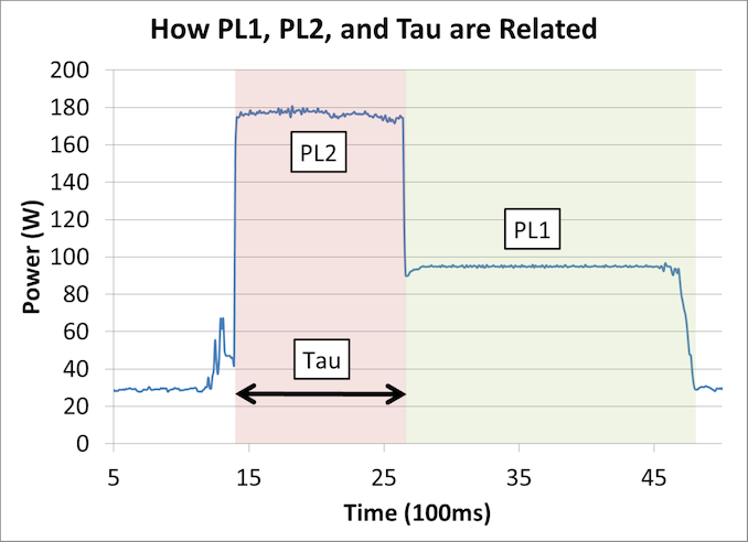
Since that post went up, additional reports have been circulating about instability issues across various online forums and message boards. The underlying culprit has been theorized to be motherboards implementing an array of strategies to improve chip performance, including aggressive multi-core enhancement settings, "unlimited" PL2 turbo, and reduced load line calibration settings. At no point do any of these settings overclock a CPU and push it to a higher clockspeed than it's validated for, but these settings do everything possible to keep a chip at the highest clockspeed possible at all times – and in the process seem to have gone a step too far.
From "Why Intel Processors Draw More Power Than Expected: TDP and Turbo Explained"
We wrote a piece initially covering multi-core enhancement in 2012, detailing how motherboard manufacturers try to stay competitive with each other and leverage any headroom within the silicon to output the highest performance levels. And more recently, we've talked about how desktop systems with Intel chips are now regularly exceeding their rated TDPs – sometimes by extreme amounts – as motherboard vendors continue to push them to run as hard as possible for the best performance.
But things have changed since 2012. At the time, this wasn't so much of an issue, as overclocking was actually very favorable to increasing the performance of processors. But in 2024 with chips such as the Intel Core i9-14900K, we have CPUs shipping with a maximum turbo clock speed of 6.0 GHz and a peak power consumption of over 400 Watts, figures that were only a pipe dream a decade ago.
Jumping to the present time, over the weekend Intel released a statement about the matter to its partners, outlining their investigation so far and their sug... CPUs

Standard CPU coolers, while adequate for managing basic thermal loads, often fall short in terms of noise reduction and superior cooling efficiency. This limitation drives advanced users and system builders to seek aftermarket solutions tailored to their specific needs. The high-end aftermarket cooler market is highly competitive, with manufacturers striving to offer products with exceptional performance.
Endorfy, previously known as SilentiumPC, is a Polish manufacturer that has undergone a significant transformation to expand its presence in global markets. The brand is known for delivering high-performance cooling solutions with a strong focus on balancing efficiency and affordability. By rebranding as Endorfy, the company aims to enter premium market segments while continuing to offer reliable, high-quality cooling products.
SilentiumPC became very popular in the value/mainstream segments of the PC market with their products, the spearhead of which probably was the Fera 5 cooler that we reviewed a little over two years ago and had a remarkable value for money. Today’s review places Endorfy’s largest CPU cooler, the Fortis 5 Dual Fan, on our laboratory test bench. The Fortis 5 is the largest CPU air cooler the company currently offers and is significantly more expensive than the Fera 5, yet it still is a single-tower cooler that strives to strike a balance between value, compatibility, and performance.
Cases/Cooling/PSUs![Micron: U.S. Fabs Will Start Operating in 2026 - 2029 <p align="center"><a href="https://www.anandtech.com/show/21459/micron-u-s-fabs-will-start-operating-in-2026-2029"><img src="https://images.anandtech.com/doci/21459/micron-server-datacenter-general-generic-678_575px.jpg" alt="" /></a></p><p><p>When Micron announced plans to build two new fabs in the U.S. in 2022, the company vaguely said both would come online by the decade's end. Then, in 2023, it began to optimize its spending, which pushed production at these fabrication facilities. This week, the company outlined more precise timeframes for when its fabs in <a href="https://www.anandtech.com/show/17573/micron-breaks-ground-on-its-15-billion-euv-dram-fab-in-the-us">Idaho</a> and <a href="https://www.anandtech.com/show/17606/micron-announces-100-billion-us-fab-complex-a-20year-plan">New York</a> will start operations: this will happen from calendar 2026 to calendar 2029.</p>
<p>"<em>These fab construction investments are necessary to support supply growth for the latter half of this decade,</em>" a statement by Micron in its Q3 FY2024 financial results report <a href="https://investors.micron.com/static-files/a531c7f0-fca2-48f3-8f24-79c945aaa2d2">reads</a>. "<em>This Idaho fab will not contribute to meaningful bit supply until fiscal 2027 and the New York construction capex is not expected to contribute to bit supply growth until fiscal 2028 or later. The timing of future [wafer fab equipment] spend in these fabs will be managed to align supply growth with expected demand growth.</em>"</p>
<p>Micron's fiscal year 2027 starts in September 2026, so the new fab near Boise, Idaho, is set to start operations between September 2026 and September 2027. The company's fiscal 2028 starts in September 2027, so the fab will likely begin operations in calendar 2028 or later, probably depending on the demand for DRAM memory in the coming years. That said, Micron's U.S. memory fabs will begin operations between late 2026 and 2029, which aligns with the company's original plans. </p>
<p>Construction of the fab in Idaho is well underway. In contrast, construction of the New York facility has yet to begin as the company is working on regulatory and permitting processes in the state. </p>
<p>Micron's capital expenditure (CaPex) plan for FY2024 is approximately $8.0 billion, with a decrease in year-over-year spending on wafer fabrication equipment (WFE). In Q4 FY2024, the company will spend around $3 billion on fab construction, new wafer fab tools, and various expansions/upgrades.</p>
<p>Looking ahead to FY2025, the company plans a substantial increase in capex, targeting a mid-30s percentage of revenue to support various technological and facility advancements. In particular, it expects its quarterly CapEx to average above the $3 billion level seen in the fourth quarter of FY2024, which means that it plans to spend about $12 billion in its fiscal 2025, which begins in late September.</p>
<p>Half or more of the total CapEx increase in FY2025 (i.e., over $2 billion) will be allocated to constructing new fabs in Idaho and New York. Meanwhile, the FY2025 CapEx will significantly rise to fund high-bandwidth memory (HBM) assembly and testing and the construction of fabrication and back-end facilities. This increase also includes investments in technology transitions to meet growing demand. </p>
<p>"<em>Fab construction in Idaho is underway, and we are working diligently to complete the regulatory and permitting processes in New York,</em>" said Sanjay Mehrotra, chief executive officer of Micron, at the company's conference call with investors and financial analysts (via <a href="https://seekingalpha.com/article/4701253-micron-technology-inc-mu-q3-2024-earnings-call-transcript?source=content_type%3Areact%7Csection%3ATranscripts%7Csection_asset%3ATranscripts%7Cfirst_level_url%3Asymbol%7Cbutton%3ATitle%7Clock_status%3ANo%7Cline%3A1">SeekingAlpha</a>). "<em>This additional leading-edge greenfield capacity, along with continued technology transition investments in our Asia facilities, is required to meet long-term demand in the second half of this decade and beyond. These investments support our objective to maintain our current bit share over time and to grow our memory bit supply in line with long-term industry bit demand.</em>"</p>
</p> Memory](https://lh3.googleusercontent.com/blogger_img_proxy/AEn0k_vqYF-ECY4Iuubc0BlzNTZ9O6tyNLJ0NYV_C9QhM8S3fONFCUiRnooZBsrXSytpFzGuR6rGkUHerbFWSw-7TKYzPaREoZG5uTy0BWxtlK5FZSd93bEzdZCl0emmxCvY5HoDpeXGq5e918nX7tOwWjz8OatrLpOeSp5nJY54tQThNG4=w72-h72-p-k-no-nu)

When Micron announced plans to build two new fabs in the U.S. in 2022, the company vaguely said both would come online by the decade's end. Then, in 2023, it began to optimize its spending, which pushed production at these fabrication facilities. This week, the company outlined more precise timeframes for when its fabs in Idaho and New York will start operations: this will happen from calendar 2026 to calendar 2029.
"These fab construction investments are necessary to support supply growth for the latter half of this decade," a statement by Micron in its Q3 FY2024 financial results report reads. "This Idaho fab will not contribute to meaningful bit supply until fiscal 2027 and the New York construction capex is not expected to contribute to bit supply growth until fiscal 2028 or later. The timing of future [wafer fab equipment] spend in these fabs will be managed to align supply growth with expected demand growth."
Micron's fiscal year 2027 starts in September 2026, so the new fab near Boise, Idaho, is set to start operations between September 2026 and September 2027. The company's fiscal 2028 starts in September 2027, so the fab will likely begin operations in calendar 2028 or later, probably depending on the demand for DRAM memory in the coming years. That said, Micron's U.S. memory fabs will begin operations between late 2026 and 2029, which aligns with the company's original plans.
Construction of the fab in Idaho is well underway. In contrast, construction of the New York facility has yet to begin as the company is working on regulatory and permitting processes in the state.
Micron's capital expenditure (CaPex) plan for FY2024 is approximately $8.0 billion, with a decrease in year-over-year spending on wafer fabrication equipment (WFE). In Q4 FY2024, the company will spend around $3 billion on fab construction, new wafer fab tools, and various expansions/upgrades.
Looking ahead to FY2025, the company plans a substantial increase in capex, targeting a mid-30s percentage of revenue to support various technological and facility advancements. In particular, it expects its quarterly CapEx to average above the $3 billion level seen in the fourth quarter of FY2024, which means that it plans to spend about $12 billion in its fiscal 2025, which begins in late September.
Half or more of the total CapEx increase in FY2025 (i.e., over $2 billion) will be allocated to constructing new fabs in Idaho and New York. Meanwhile, the FY2025 CapEx will significantly rise to fund high-bandwidth memory (HBM) assembly and testing and the construction of fabrication and back-end facilities. This increase also includes investments in technology transitions to meet growing demand.
"Fab construction in Idaho is underway, and we are working diligently to complete the regulatory and permitting processes in New York," said Sanjay Mehrotra, chief executive officer of Micron, at the company's conference call with investors and financial analysts (via SeekingAlpha). "This additional leading-edge greenfield capacity, along with continued technology transition investments in our Asia facilities, is required to meet long-term demand in the second half of this decade and beyond. These investments support our objective to maintain our current bit share over time and to grow our memory bit supply in line with long-term industry bit demand."
Memory

Kioxia's booth at FMS 2024 was a busy one with multiple technology demonstrations keeping visitors occupied. A walk-through of the BiCS 8 manufacturing process was the first to grab my attention. Kioxia and Western Digital announced the sampling of BiCS 8 in March 2023. We had touched briefly upon its CMOS Bonded Array (CBA) scheme in our coverage of Kioxial's 2Tb QLC NAND device and coverage of Western Digital's 128 TB QLC enterprise SSD proof-of-concept demonstration. At Kioxia's booth, we got more insights.

Traditionally, fabrication of flash chips involved placement of the associate logic circuitry (CMOS process) around the periphery of the flash array. The process then moved on to putting the CMOS under the cell array, but the wafer development process was serialized with the CMOS logic getting fabricated first followed by the cell array on top. However, this has some challenges because the cell array requires a high-temperature processing step to ensure higher reliability that can be detrimental to the health of the CMOS logic. Thanks to recent advancements in wafer bonding techniques, the new CBA process allows the CMOS wafer and cell array wafer to be processed independently in parallel and then pieced together, as shown in the models above.

The BiCS 8 3D NAND incorporates 218 layers, compared to 112 layers in BiCS 5 and 162 layers in BiCS 6. The company decided to skip over BiCS 7 (or, rather, it was probably a short-lived generation meant as an internal test vehicle). The generation retains the four-plane charge trap structure of BiCS 6. In its TLC avatar, it is available as a 1 Tbit device. The QLC version is available in two capacities - 1 Tbit and 2 Tbit.
Kioxia also noted that while the number of layers (218) doesn't compare favorably with the latest layer counts from the competition, its lateral scaling / cell shrinkage has enabled it to be competitive in terms of bit density as well as operating speeds (3200 MT/s). For reference, the latest shipping NAND from Micron - the G9 - has 276 layers with a bit density in TLC mode of 21 Gbit/mm2, and operates at up to 3600 MT/s. However, its 232L NAND operates only up to 2400 MT/s and has a bit density of 14.6 Gbit/mm2.
It must be noted that the CBA hybrid bonding process has advantages over the current processes used by other vendors - including Micron's CMOS under array (CuA) and SK hynix's 4D PUC (periphery-under-chip) developed in the late 2010s. It is expected that other NAND vendors will also move eventually to some variant of the hybrid bonding scheme used by Kioxia.
Storage
Lorem Ipsum is simply dummy text of the printing and typesetting industry. Lorem Ipsum has been the industry's.


 and raised power consumption limits that seek to maximize how hard and how long systems are able to turbo boost – the issue has finally come to a head in the last couple of months thanks to accumulating reports of system instability with Intel's 13900K and 14900K processors. These instability problems are eventually solved by either tamping down on these motherboard performance-boosting features – bringing the chips back down to something closer to Intel's official operating parameters – or downclocking the chips entirely.</p>
<p>Intel first began publicly investigating the matter on the 27th of February, when Intel's Communications Manager, Thomas Hannaford, posted a thread on Intel's Community Product Support Forms titled "Regarding Reports of 13th/14th Gen Unlocked Desktop Users Experiencing Stability Issues". In this thread, Thomas Hannaford said, "<em>Intel is aware of reports regarding Intel Core 13th and 14th Gen unlocked desktop processors experiencing issues with certain workloads. We're engaged with our partners and are conducting analysis of the reported issues. If you are experiencing these issues, please reach out to Intel Customer Support for further assistance in the interim.</em>"</p>
<p>Since that post went up, additional reports have been circulating about instability issues across various online forums and message boards. The underlying culprit has been theorized to be motherboards implementing an array of strategies to improve chip performance, including aggressive multi-core enhancement settings, "unlimited" PL2 turbo, and reduced load line calibration settings. At no point do any of these settings overclock a CPU and push it to a higher clockspeed than it's validated for, but these settings do everything possible to keep a chip at the highest clockspeed possible at all times – and in the process seem to have gone a step too far.</p>
<p align="center"><a href="https://www.anandtech.com/show/21374/intel-issues-request-to-mobo-vendors-to-use-stock-power-settings-for-stability"><img alt="" src="https://images.anandtech.com/doci/21374/95WTau_575px.png" /></a><br />
<small><em>From "<a href="https://www.anandtech.com/show/13544/why-intel-processors-draw-more-power-than-expected-tdp-turbo">Why Intel Processors Draw More Power Than Expected: TDP and Turbo Explained</a>"</em></small></p>
<p><a href="https://www.anandtech.com/show/6214/multicore-enhancement-the-debate-about-free-mhz">We wrote a piece initially covering multi-core enhancement in 2012</a>, detailing how motherboard manufacturers try to stay competitive with each other and leverage any headroom within the silicon to output the highest performance levels. And more recently, <a href="https://www.anandtech.com/show/13544/why-intel-processors-draw-more-power-than-expected-tdp-turbo">we've talked about how desktop systems with Intel chips are now regularly exceeding their rated TDPs</a> – sometimes by extreme amounts – as motherboard vendors continue to push them to run as hard as possible for the best performance.</p>
<p>But things have changed since 2012. At the time, this wasn't so much of an issue, as overclocking was actually very favorable to increasing the performance of processors. But in 2024 with chips such as the Intel Core i9-14900K, we have CPUs shipping with a maximum turbo clock speed of 6.0 GHz and a peak power consumption of over <a href="https://www.anandtech.com/show/21084/intel-core-i9-14900k-core-i7-14700k-and-core-i5-14600k-review-raptor-lake-refreshed/6">400 Watts</a>, figures that were only a pipe dream a decade ago.</p>
<p>Jumping to the present time, over the weekend Intel released a statement about the matter to its partners, outlining their investigation so far and their sug... CPUs)
 and raised power consumption limits that seek to maximize how hard and how long systems are able to turbo boost – the issue has finally come to a head in the last couple of months thanks to accumulating reports of system instability with Intel's 13900K and 14900K processors. These instability problems are eventually solved by either tamping down on these motherboard performance-boosting features – bringing the chips back down to something closer to Intel's official operating parameters – or downclocking the chips entirely.</p>
<p>Intel first began publicly investigating the matter on the 27th of February, when Intel's Communications Manager, Thomas Hannaford, posted a thread on Intel's Community Product Support Forms titled "Regarding Reports of 13th/14th Gen Unlocked Desktop Users Experiencing Stability Issues". In this thread, Thomas Hannaford said, "<em>Intel is aware of reports regarding Intel Core 13th and 14th Gen unlocked desktop processors experiencing issues with certain workloads. We're engaged with our partners and are conducting analysis of the reported issues. If you are experiencing these issues, please reach out to Intel Customer Support for further assistance in the interim.</em>"</p>
<p>Since that post went up, additional reports have been circulating about instability issues across various online forums and message boards. The underlying culprit has been theorized to be motherboards implementing an array of strategies to improve chip performance, including aggressive multi-core enhancement settings, "unlimited" PL2 turbo, and reduced load line calibration settings. At no point do any of these settings overclock a CPU and push it to a higher clockspeed than it's validated for, but these settings do everything possible to keep a chip at the highest clockspeed possible at all times – and in the process seem to have gone a step too far.</p>
<p align="center"><a href="https://www.anandtech.com/show/21374/intel-issues-request-to-mobo-vendors-to-use-stock-power-settings-for-stability"><img alt="" src="https://images.anandtech.com/doci/21374/95WTau_575px.png" /></a><br />
<small><em>From "<a href="https://www.anandtech.com/show/13544/why-intel-processors-draw-more-power-than-expected-tdp-turbo">Why Intel Processors Draw More Power Than Expected: TDP and Turbo Explained</a>"</em></small></p>
<p><a href="https://www.anandtech.com/show/6214/multicore-enhancement-the-debate-about-free-mhz">We wrote a piece initially covering multi-core enhancement in 2012</a>, detailing how motherboard manufacturers try to stay competitive with each other and leverage any headroom within the silicon to output the highest performance levels. And more recently, <a href="https://www.anandtech.com/show/13544/why-intel-processors-draw-more-power-than-expected-tdp-turbo">we've talked about how desktop systems with Intel chips are now regularly exceeding their rated TDPs</a> – sometimes by extreme amounts – as motherboard vendors continue to push them to run as hard as possible for the best performance.</p>
<p>But things have changed since 2012. At the time, this wasn't so much of an issue, as overclocking was actually very favorable to increasing the performance of processors. But in 2024 with chips such as the Intel Core i9-14900K, we have CPUs shipping with a maximum turbo clock speed of 6.0 GHz and a peak power consumption of over <a href="https://www.anandtech.com/show/21084/intel-core-i9-14900k-core-i7-14700k-and-core-i5-14600k-review-raptor-lake-refreshed/6">400 Watts</a>, figures that were only a pipe dream a decade ago.</p>
<p>Jumping to the present time, over the weekend Intel released a statement about the matter to its partners, outlining their investigation so far and their sug... CPUs | https://compbuddey.blogspot.com/2024/05/in-light-of-stability-concerns-intel.html)
 and raised power consumption limits that seek to maximize how hard and how long systems are able to turbo boost – the issue has finally come to a head in the last couple of months thanks to accumulating reports of system instability with Intel's 13900K and 14900K processors. These instability problems are eventually solved by either tamping down on these motherboard performance-boosting features – bringing the chips back down to something closer to Intel's official operating parameters – or downclocking the chips entirely.</p>
<p>Intel first began publicly investigating the matter on the 27th of February, when Intel's Communications Manager, Thomas Hannaford, posted a thread on Intel's Community Product Support Forms titled "Regarding Reports of 13th/14th Gen Unlocked Desktop Users Experiencing Stability Issues". In this thread, Thomas Hannaford said, "<em>Intel is aware of reports regarding Intel Core 13th and 14th Gen unlocked desktop processors experiencing issues with certain workloads. We're engaged with our partners and are conducting analysis of the reported issues. If you are experiencing these issues, please reach out to Intel Customer Support for further assistance in the interim.</em>"</p>
<p>Since that post went up, additional reports have been circulating about instability issues across various online forums and message boards. The underlying culprit has been theorized to be motherboards implementing an array of strategies to improve chip performance, including aggressive multi-core enhancement settings, "unlimited" PL2 turbo, and reduced load line calibration settings. At no point do any of these settings overclock a CPU and push it to a higher clockspeed than it's validated for, but these settings do everything possible to keep a chip at the highest clockspeed possible at all times – and in the process seem to have gone a step too far.</p>
<p align="center"><a href="https://www.anandtech.com/show/21374/intel-issues-request-to-mobo-vendors-to-use-stock-power-settings-for-stability"><img alt="" src="https://images.anandtech.com/doci/21374/95WTau_575px.png" /></a><br />
<small><em>From "<a href="https://www.anandtech.com/show/13544/why-intel-processors-draw-more-power-than-expected-tdp-turbo">Why Intel Processors Draw More Power Than Expected: TDP and Turbo Explained</a>"</em></small></p>
<p><a href="https://www.anandtech.com/show/6214/multicore-enhancement-the-debate-about-free-mhz">We wrote a piece initially covering multi-core enhancement in 2012</a>, detailing how motherboard manufacturers try to stay competitive with each other and leverage any headroom within the silicon to output the highest performance levels. And more recently, <a href="https://www.anandtech.com/show/13544/why-intel-processors-draw-more-power-than-expected-tdp-turbo">we've talked about how desktop systems with Intel chips are now regularly exceeding their rated TDPs</a> – sometimes by extreme amounts – as motherboard vendors continue to push them to run as hard as possible for the best performance.</p>
<p>But things have changed since 2012. At the time, this wasn't so much of an issue, as overclocking was actually very favorable to increasing the performance of processors. But in 2024 with chips such as the Intel Core i9-14900K, we have CPUs shipping with a maximum turbo clock speed of 6.0 GHz and a peak power consumption of over <a href="https://www.anandtech.com/show/21084/intel-core-i9-14900k-core-i7-14700k-and-core-i5-14600k-review-raptor-lake-refreshed/6">400 Watts</a>, figures that were only a pipe dream a decade ago.</p>
<p>Jumping to the present time, over the weekend Intel released a statement about the matter to its partners, outlining their investigation so far and their sug... CPUs&body=https://compbuddey.blogspot.com/2024/05/in-light-of-stability-concerns-intel.html)
0 Comments