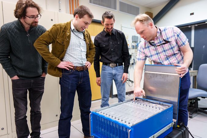

While neuromorphic computing remains under research for the time being, efforts into the field have continued to grow over the years, as have the capabilities of the specialty chips that have been developed for this research. Following those lines, this morning Intel and Sandia National Laboratories are celebrating the deployment of the Hala Point neuromorphic system, which the two believe is the highest capacity system in the world. With 1.15 billion neurons overall, Hala Point is the largest deployment yet for Intel’s Loihi 2 neuromorphic chip, which was first announced at the tail-end of 2021.
The Hala Point system incorporates 1152 Loihi 2 processors, each of which is capable of simulating a million neurons. As noted back at the time of Loihi 2’s launch, these chips are actually rather small – just 31 mm2 per chip with 2.3 billion transistors each, as they’re built on the Intel 4 process (one of the only other Intel chips to do so, besides Meteor Lake). As a result, the complete system is similarly petite, taking up just 6 rack units of space (or as Sandia likes to compare it to, about the size of a microwave), with a power consumption of 2.6 kW. Now that it’s online, Hala Point has dethroned the SpiNNaker system as the largest disclosed neuromorphic system, offering admittedly just a slightly larger number of neurons at less than 3% of the power consumption of the 100 kW British system.
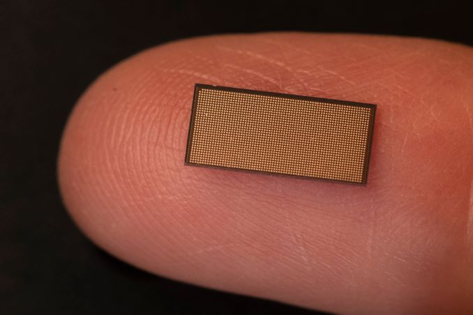
A Single Loihi 2 Chip (31 mm2)
Hala Point will be replacing an older Intel neuromorphic system at Sandia, Pohoiki Springs, which is based on Intel’s first-generation Loihi chips. By comparison, Hala Point offers ten-times as many neurons, and upwards of 12x the performance overall,
Both neuromorphic systems have been procured by Sandia in order to advance the national lab’s research into neuromorphic computing, a computing paradigm that behaves like a brain. The central thought (if you’ll excuse the pun) is that by mimicking the wetware writing this article, neuromorphic chips can be used to solve problems that conventional processors cannot solve today, and that they can do so more efficiently as well.
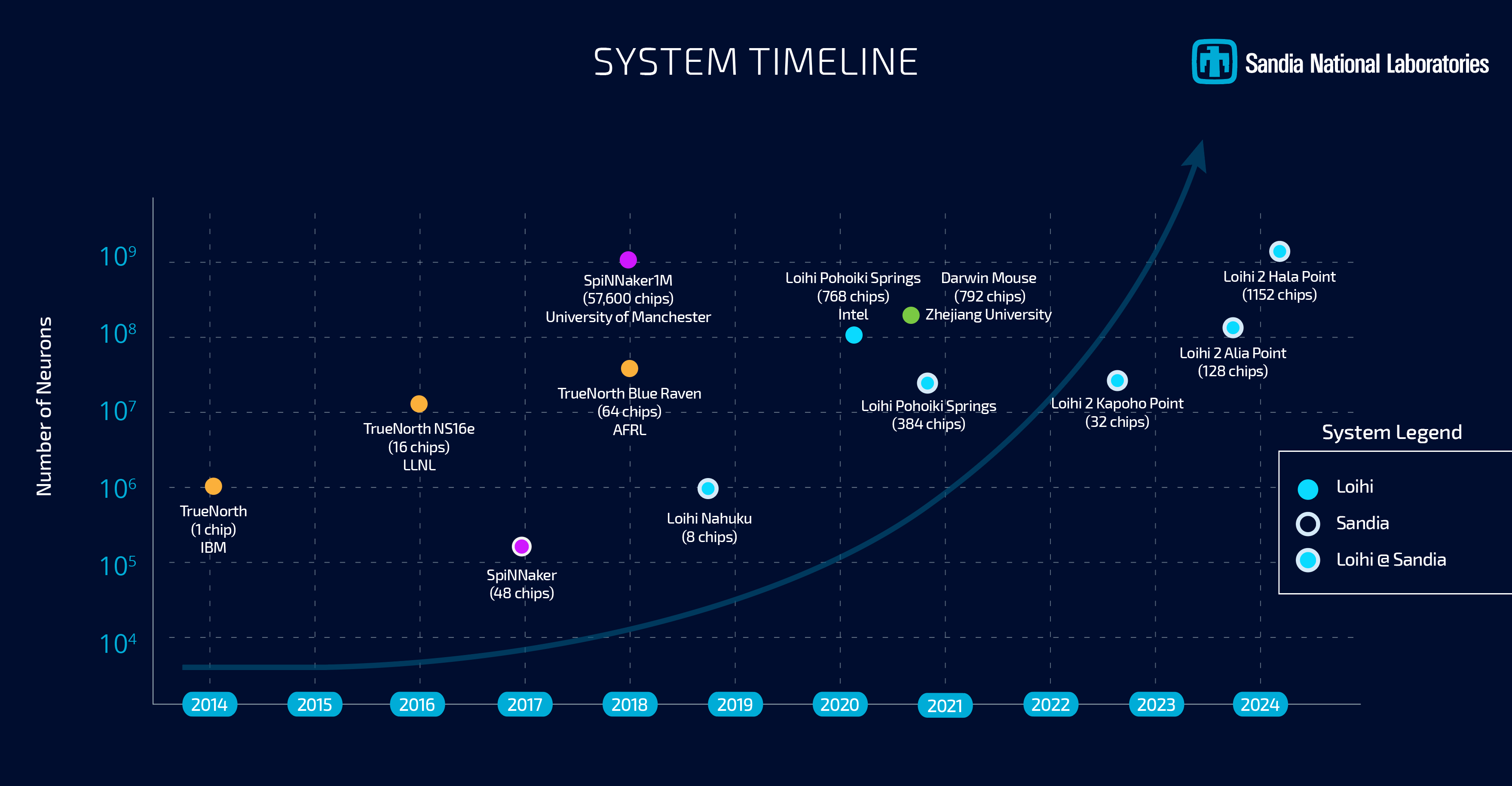
Sandia, for its part, has said that it will be using the system to look at large-scale neuromorphic computing, with work operating on a scale well beyond Pohoiki Springs. With Hala Point offering a simulated neuron count very roughly on the level of complexity of an owl brain, the lab believes that a larger-scale system will finally enable them to properly exploit the properties of neuromorphic computing to solve real problems in fields such as device physics, computer architecture, computer science and informatics, moving well beyond the simple demonstrations initially achieved at a smaller scale.
One new focus from the lab, which in turn has caught Intel’s attention, is the applicability of neuromorphic computing towards AI inference. Because the neural networks themselves behind the current wave of AI systems are attempting to emulate the human brain, in a sense, there is an obvious degree of synergy with the brain-mimicking neuromorphic chips, even if the algorithms differ in some key respects. Still, with energy efficiency being one of the major benefits of neuromorphic computing, it’s pushed Intel to look into the matter further – and even build a second, Hala Point-sized system of their own.
According to Intel, in their research on Hala Point, the system has reached efficiencies as high as 15 TOPS-per-Watt at 8-bit precision, albeit while using 10:1 sparsity, making it more than competitive with current-generation commercial chips. As an added bonus to that efficiency, the neuromorphic systems don’t require extensive data processing and batching in advance, which is normally necessary to make efficient use of the high density ALU arrays in GPUs and GPU-like processors.
Perhaps the most interesting use case of all, however, is the potent... CPUs
![Micron: U.S. Fabs Will Start Operating in 2026 - 2029 <p align="center"><a href="https://www.anandtech.com/show/21459/micron-u-s-fabs-will-start-operating-in-2026-2029"><img src="https://images.anandtech.com/doci/21459/micron-server-datacenter-general-generic-678_575px.jpg" alt="" /></a></p><p><p>When Micron announced plans to build two new fabs in the U.S. in 2022, the company vaguely said both would come online by the decade's end. Then, in 2023, it began to optimize its spending, which pushed production at these fabrication facilities. This week, the company outlined more precise timeframes for when its fabs in <a href="https://www.anandtech.com/show/17573/micron-breaks-ground-on-its-15-billion-euv-dram-fab-in-the-us">Idaho</a> and <a href="https://www.anandtech.com/show/17606/micron-announces-100-billion-us-fab-complex-a-20year-plan">New York</a> will start operations: this will happen from calendar 2026 to calendar 2029.</p>
<p>"<em>These fab construction investments are necessary to support supply growth for the latter half of this decade,</em>" a statement by Micron in its Q3 FY2024 financial results report <a href="https://investors.micron.com/static-files/a531c7f0-fca2-48f3-8f24-79c945aaa2d2">reads</a>. "<em>This Idaho fab will not contribute to meaningful bit supply until fiscal 2027 and the New York construction capex is not expected to contribute to bit supply growth until fiscal 2028 or later. The timing of future [wafer fab equipment] spend in these fabs will be managed to align supply growth with expected demand growth.</em>"</p>
<p>Micron's fiscal year 2027 starts in September 2026, so the new fab near Boise, Idaho, is set to start operations between September 2026 and September 2027. The company's fiscal 2028 starts in September 2027, so the fab will likely begin operations in calendar 2028 or later, probably depending on the demand for DRAM memory in the coming years. That said, Micron's U.S. memory fabs will begin operations between late 2026 and 2029, which aligns with the company's original plans. </p>
<p>Construction of the fab in Idaho is well underway. In contrast, construction of the New York facility has yet to begin as the company is working on regulatory and permitting processes in the state. </p>
<p>Micron's capital expenditure (CaPex) plan for FY2024 is approximately $8.0 billion, with a decrease in year-over-year spending on wafer fabrication equipment (WFE). In Q4 FY2024, the company will spend around $3 billion on fab construction, new wafer fab tools, and various expansions/upgrades.</p>
<p>Looking ahead to FY2025, the company plans a substantial increase in capex, targeting a mid-30s percentage of revenue to support various technological and facility advancements. In particular, it expects its quarterly CapEx to average above the $3 billion level seen in the fourth quarter of FY2024, which means that it plans to spend about $12 billion in its fiscal 2025, which begins in late September.</p>
<p>Half or more of the total CapEx increase in FY2025 (i.e., over $2 billion) will be allocated to constructing new fabs in Idaho and New York. Meanwhile, the FY2025 CapEx will significantly rise to fund high-bandwidth memory (HBM) assembly and testing and the construction of fabrication and back-end facilities. This increase also includes investments in technology transitions to meet growing demand. </p>
<p>"<em>Fab construction in Idaho is underway, and we are working diligently to complete the regulatory and permitting processes in New York,</em>" said Sanjay Mehrotra, chief executive officer of Micron, at the company's conference call with investors and financial analysts (via <a href="https://seekingalpha.com/article/4701253-micron-technology-inc-mu-q3-2024-earnings-call-transcript?source=content_type%3Areact%7Csection%3ATranscripts%7Csection_asset%3ATranscripts%7Cfirst_level_url%3Asymbol%7Cbutton%3ATitle%7Clock_status%3ANo%7Cline%3A1">SeekingAlpha</a>). "<em>This additional leading-edge greenfield capacity, along with continued technology transition investments in our Asia facilities, is required to meet long-term demand in the second half of this decade and beyond. These investments support our objective to maintain our current bit share over time and to grow our memory bit supply in line with long-term industry bit demand.</em>"</p>
</p> Memory](https://lh3.googleusercontent.com/blogger_img_proxy/AEn0k_sR_JAGnA-rNYXmmvFwic8w0QdpvVPo0ZqVTt5Q86TM10cWK-0uJHQ10giqr2KijbLSN8hnjIs7sfbKAm_BFfzg1988gopSWw_iHbpcf--BMIhM1F_SO1wK155s__lBZcn3jCbNWWH98Cjy7zsdFY6sQhu5VCVI7e8k0meyqrYf-xM=w72-h72-p-k-no-nu)

When Micron announced plans to build two new fabs in the U.S. in 2022, the company vaguely said both would come online by the decade's end. Then, in 2023, it began to optimize its spending, which pushed production at these fabrication facilities. This week, the company outlined more precise timeframes for when its fabs in Idaho and New York will start operations: this will happen from calendar 2026 to calendar 2029.
"These fab construction investments are necessary to support supply growth for the latter half of this decade," a statement by Micron in its Q3 FY2024 financial results report reads. "This Idaho fab will not contribute to meaningful bit supply until fiscal 2027 and the New York construction capex is not expected to contribute to bit supply growth until fiscal 2028 or later. The timing of future [wafer fab equipment] spend in these fabs will be managed to align supply growth with expected demand growth."
Micron's fiscal year 2027 starts in September 2026, so the new fab near Boise, Idaho, is set to start operations between September 2026 and September 2027. The company's fiscal 2028 starts in September 2027, so the fab will likely begin operations in calendar 2028 or later, probably depending on the demand for DRAM memory in the coming years. That said, Micron's U.S. memory fabs will begin operations between late 2026 and 2029, which aligns with the company's original plans.
Construction of the fab in Idaho is well underway. In contrast, construction of the New York facility has yet to begin as the company is working on regulatory and permitting processes in the state.
Micron's capital expenditure (CaPex) plan for FY2024 is approximately $8.0 billion, with a decrease in year-over-year spending on wafer fabrication equipment (WFE). In Q4 FY2024, the company will spend around $3 billion on fab construction, new wafer fab tools, and various expansions/upgrades.
Looking ahead to FY2025, the company plans a substantial increase in capex, targeting a mid-30s percentage of revenue to support various technological and facility advancements. In particular, it expects its quarterly CapEx to average above the $3 billion level seen in the fourth quarter of FY2024, which means that it plans to spend about $12 billion in its fiscal 2025, which begins in late September.
Half or more of the total CapEx increase in FY2025 (i.e., over $2 billion) will be allocated to constructing new fabs in Idaho and New York. Meanwhile, the FY2025 CapEx will significantly rise to fund high-bandwidth memory (HBM) assembly and testing and the construction of fabrication and back-end facilities. This increase also includes investments in technology transitions to meet growing demand.
"Fab construction in Idaho is underway, and we are working diligently to complete the regulatory and permitting processes in New York," said Sanjay Mehrotra, chief executive officer of Micron, at the company's conference call with investors and financial analysts (via SeekingAlpha). "This additional leading-edge greenfield capacity, along with continued technology transition investments in our Asia facilities, is required to meet long-term demand in the second half of this decade and beyond. These investments support our objective to maintain our current bit share over time and to grow our memory bit supply in line with long-term industry bit demand."
Memory

Kioxia's booth at FMS 2024 was a busy one with multiple technology demonstrations keeping visitors occupied. A walk-through of the BiCS 8 manufacturing process was the first to grab my attention. Kioxia and Western Digital announced the sampling of BiCS 8 in March 2023. We had touched briefly upon its CMOS Bonded Array (CBA) scheme in our coverage of Kioxial's 2Tb QLC NAND device and coverage of Western Digital's 128 TB QLC enterprise SSD proof-of-concept demonstration. At Kioxia's booth, we got more insights.

Traditionally, fabrication of flash chips involved placement of the associate logic circuitry (CMOS process) around the periphery of the flash array. The process then moved on to putting the CMOS under the cell array, but the wafer development process was serialized with the CMOS logic getting fabricated first followed by the cell array on top. However, this has some challenges because the cell array requires a high-temperature processing step to ensure higher reliability that can be detrimental to the health of the CMOS logic. Thanks to recent advancements in wafer bonding techniques, the new CBA process allows the CMOS wafer and cell array wafer to be processed independently in parallel and then pieced together, as shown in the models above.

The BiCS 8 3D NAND incorporates 218 layers, compared to 112 layers in BiCS 5 and 162 layers in BiCS 6. The company decided to skip over BiCS 7 (or, rather, it was probably a short-lived generation meant as an internal test vehicle). The generation retains the four-plane charge trap structure of BiCS 6. In its TLC avatar, it is available as a 1 Tbit device. The QLC version is available in two capacities - 1 Tbit and 2 Tbit.
Kioxia also noted that while the number of layers (218) doesn't compare favorably with the latest layer counts from the competition, its lateral scaling / cell shrinkage has enabled it to be competitive in terms of bit density as well as operating speeds (3200 MT/s). For reference, the latest shipping NAND from Micron - the G9 - has 276 layers with a bit density in TLC mode of 21 Gbit/mm2, and operates at up to 3600 MT/s. However, its 232L NAND operates only up to 2400 MT/s and has a bit density of 14.6 Gbit/mm2.
It must be noted that the CBA hybrid bonding process has advantages over the current processes used by other vendors - including Micron's CMOS under array (CuA) and SK hynix's 4D PUC (periphery-under-chip) developed in the late 2010s. It is expected that other NAND vendors will also move eventually to some variant of the hybrid bonding scheme used by Kioxia.
Storage

G.Skill on Tuesday introduced its ultra-low-latency DDR5-6400 memory modules that feature a CAS latency of 30 clocks, which appears to be the industry's most aggressive timings yet for DDR5-6400 sticks. The modules will be available for both AMD and Intel CPU-based systems.
With every new generation of DDR memory comes an increase in data transfer rates and an extension of relative latencies. While for the vast majority of applications, the increased bandwidth offsets the performance impact of higher timings, there are applications that favor low latencies. However, shrinking latencies is sometimes harder than increasing data transfer rates, which is why low-latency modules are rare.
Nonetheless, G.Skill has apparently managed to cherry-pick enough DDR5 memory chips and build appropriate printed circuit boards to produce DDR5-6400 modules with CL30 timings, which are substantially lower than the CL46 timings recommended by JEDEC for this speed bin. This means that while JEDEC-standard modules have an absolute latency of 14.375 ns, G.Skill's modules can boast a latency of just 9.375 ns – an approximately 35% decrease.
G.Skill's DDR5-6400 CL30 39-39-102 modules have a capacity of 16 GB and will be available in 32 GB dual-channel kits, though the company does not disclose voltages, which are likely considerably higher than those standardized by JEDEC.
The company plans to make its DDR5-6400 modules available both for AMD systems with EXPO profiles (Trident Z5 Neo RGB and Trident Z5 Royal Neo) and for Intel-powered PCs with XMP 3.0 profiles (Trident Z5 RGB and Trident Z5 Royal). For AMD AM5 systems that have a practical limitation of 6000 MT/s – 6400 MT/s for DDR5 memory (as this is roughly as fast as AMD's Infinity Fabric can operate at with a 1:1 ratio), the new modules will be particularly beneficial for AMD's Ryzen 7000 and Ryzen 9000-series processors.
G.Skill notes that since its modules are non-standard, they will not work with all systems but will operate on high-end motherboards with properly cooled CPUs.
The new ultra-low-latency memory kits will be available worldwide from G.Skill's partners starting in late August 2024. The company did not disclose the pricing of these modules, but since we are talking about premium products that boast unique specifications, they are likely to be priced accordingly.
Memory
Lorem Ipsum is simply dummy text of the printing and typesetting industry. Lorem Ipsum has been the industry's.


. As a result, the complete system is similarly petite, taking up just 6 rack units of space (or as Sandia likes to compare it to, about the size of a microwave), with a power consumption of 2.6 kW. Now that it’s online, Hala Point has dethroned <a href="http://apt.cs.manchester.ac.uk/projects/SpiNNaker/">the SpiNNaker system</a> as the largest disclosed neuromorphic system, offering admittedly just a slightly larger number of neurons at less than 3% of the power consumption of the 100 kW British system.</p>
<p align="center"><a href="https://www.anandtech.com/show/21355/intel-and-sandia-national-laboratories-roll-out-hala-point-neuromorphic-research-system"><img alt="" src="https://images.anandtech.com/doci/21355/LoihiFingertip3000_575px.jpg" /></a><br />
<small><em>A Single Loihi 2 Chip (31 mm<sup>2</sup>)</em></small></p>
<p>Hala Point will be replacing an older Intel neuromorphic system at Sandia, Pohoiki Springs, which is based on Intel’s first-generation Loihi chips. By comparison, Hala Point offers ten-times as many neurons, and upwards of 12x the performance overall,</p>
<p>Both neuromorphic systems have been procured by Sandia in order to advance the national lab’s research into neuromorphic computing, a computing paradigm that behaves like a brain. The central thought (if you’ll excuse the pun) is that by mimicking the wetware writing this article, neuromorphic chips can be used to solve problems that conventional processors cannot solve today, and that they can do so more efficiently as well.</p>
<p align="center"><a href="https://www.anandtech.com/show/21355/intel-and-sandia-national-laboratories-roll-out-hala-point-neuromorphic-research-system"><img alt="" src="https://images.anandtech.com/doci/21355/LOIHI_Chart-final.png" style="width: 100%;" /></a></p>
<p>Sandia, for its part, has said that it will be using the system to look at large-scale neuromorphic computing, with work operating on a scale well beyond Pohoiki Springs. With Hala Point offering a simulated neuron count very roughly on the level of complexity of an owl brain, the lab believes that a larger-scale system will finally enable them to properly exploit the properties of neuromorphic computing to solve real problems in fields such as device physics, computer architecture, computer science and informatics, moving well beyond the simple demonstrations initially achieved at a smaller scale.</p>
<p>One new focus from the lab, which in turn has caught Intel’s attention, is the applicability of neuromorphic computing towards AI inference. Because the neural networks themselves behind the current wave of AI systems are attempting to emulate the human brain, in a sense, there is an obvious degree of synergy with the brain-mimicking neuromorphic chips, even if the algorithms differ in some key respects. Still, with energy efficiency being one of the major benefits of neuromorphic computing, it’s pushed Intel to look into the matter further – and even build a second, Hala Point-sized system of their own.</p>
<p>According to Intel, in their research on Hala Point, the system has reached efficiencies as high as 15 TOPS-per-Watt at 8-bit precision, albeit while using 10:1 sparsity, making it more than competitive with current-generation commercial chips. As an added bonus to that efficiency, the neuromorphic systems don’t require extensive data processing and batching in advance, which is normally necessary to make efficient use of the high density ALU arrays in GPUs and GPU-like processors.</p>
<p>Perhaps the most interesting use case of all, however, is the potent... CPUs)
. As a result, the complete system is similarly petite, taking up just 6 rack units of space (or as Sandia likes to compare it to, about the size of a microwave), with a power consumption of 2.6 kW. Now that it’s online, Hala Point has dethroned <a href="http://apt.cs.manchester.ac.uk/projects/SpiNNaker/">the SpiNNaker system</a> as the largest disclosed neuromorphic system, offering admittedly just a slightly larger number of neurons at less than 3% of the power consumption of the 100 kW British system.</p>
<p align="center"><a href="https://www.anandtech.com/show/21355/intel-and-sandia-national-laboratories-roll-out-hala-point-neuromorphic-research-system"><img alt="" src="https://images.anandtech.com/doci/21355/LoihiFingertip3000_575px.jpg" /></a><br />
<small><em>A Single Loihi 2 Chip (31 mm<sup>2</sup>)</em></small></p>
<p>Hala Point will be replacing an older Intel neuromorphic system at Sandia, Pohoiki Springs, which is based on Intel’s first-generation Loihi chips. By comparison, Hala Point offers ten-times as many neurons, and upwards of 12x the performance overall,</p>
<p>Both neuromorphic systems have been procured by Sandia in order to advance the national lab’s research into neuromorphic computing, a computing paradigm that behaves like a brain. The central thought (if you’ll excuse the pun) is that by mimicking the wetware writing this article, neuromorphic chips can be used to solve problems that conventional processors cannot solve today, and that they can do so more efficiently as well.</p>
<p align="center"><a href="https://www.anandtech.com/show/21355/intel-and-sandia-national-laboratories-roll-out-hala-point-neuromorphic-research-system"><img alt="" src="https://images.anandtech.com/doci/21355/LOIHI_Chart-final.png" style="width: 100%;" /></a></p>
<p>Sandia, for its part, has said that it will be using the system to look at large-scale neuromorphic computing, with work operating on a scale well beyond Pohoiki Springs. With Hala Point offering a simulated neuron count very roughly on the level of complexity of an owl brain, the lab believes that a larger-scale system will finally enable them to properly exploit the properties of neuromorphic computing to solve real problems in fields such as device physics, computer architecture, computer science and informatics, moving well beyond the simple demonstrations initially achieved at a smaller scale.</p>
<p>One new focus from the lab, which in turn has caught Intel’s attention, is the applicability of neuromorphic computing towards AI inference. Because the neural networks themselves behind the current wave of AI systems are attempting to emulate the human brain, in a sense, there is an obvious degree of synergy with the brain-mimicking neuromorphic chips, even if the algorithms differ in some key respects. Still, with energy efficiency being one of the major benefits of neuromorphic computing, it’s pushed Intel to look into the matter further – and even build a second, Hala Point-sized system of their own.</p>
<p>According to Intel, in their research on Hala Point, the system has reached efficiencies as high as 15 TOPS-per-Watt at 8-bit precision, albeit while using 10:1 sparsity, making it more than competitive with current-generation commercial chips. As an added bonus to that efficiency, the neuromorphic systems don’t require extensive data processing and batching in advance, which is normally necessary to make efficient use of the high density ALU arrays in GPUs and GPU-like processors.</p>
<p>Perhaps the most interesting use case of all, however, is the potent... CPUs | https://compbuddey.blogspot.com/2024/04/intel-and-sandia-national-labs-roll-out_27.html)
. As a result, the complete system is similarly petite, taking up just 6 rack units of space (or as Sandia likes to compare it to, about the size of a microwave), with a power consumption of 2.6 kW. Now that it’s online, Hala Point has dethroned <a href="http://apt.cs.manchester.ac.uk/projects/SpiNNaker/">the SpiNNaker system</a> as the largest disclosed neuromorphic system, offering admittedly just a slightly larger number of neurons at less than 3% of the power consumption of the 100 kW British system.</p>
<p align="center"><a href="https://www.anandtech.com/show/21355/intel-and-sandia-national-laboratories-roll-out-hala-point-neuromorphic-research-system"><img alt="" src="https://images.anandtech.com/doci/21355/LoihiFingertip3000_575px.jpg" /></a><br />
<small><em>A Single Loihi 2 Chip (31 mm<sup>2</sup>)</em></small></p>
<p>Hala Point will be replacing an older Intel neuromorphic system at Sandia, Pohoiki Springs, which is based on Intel’s first-generation Loihi chips. By comparison, Hala Point offers ten-times as many neurons, and upwards of 12x the performance overall,</p>
<p>Both neuromorphic systems have been procured by Sandia in order to advance the national lab’s research into neuromorphic computing, a computing paradigm that behaves like a brain. The central thought (if you’ll excuse the pun) is that by mimicking the wetware writing this article, neuromorphic chips can be used to solve problems that conventional processors cannot solve today, and that they can do so more efficiently as well.</p>
<p align="center"><a href="https://www.anandtech.com/show/21355/intel-and-sandia-national-laboratories-roll-out-hala-point-neuromorphic-research-system"><img alt="" src="https://images.anandtech.com/doci/21355/LOIHI_Chart-final.png" style="width: 100%;" /></a></p>
<p>Sandia, for its part, has said that it will be using the system to look at large-scale neuromorphic computing, with work operating on a scale well beyond Pohoiki Springs. With Hala Point offering a simulated neuron count very roughly on the level of complexity of an owl brain, the lab believes that a larger-scale system will finally enable them to properly exploit the properties of neuromorphic computing to solve real problems in fields such as device physics, computer architecture, computer science and informatics, moving well beyond the simple demonstrations initially achieved at a smaller scale.</p>
<p>One new focus from the lab, which in turn has caught Intel’s attention, is the applicability of neuromorphic computing towards AI inference. Because the neural networks themselves behind the current wave of AI systems are attempting to emulate the human brain, in a sense, there is an obvious degree of synergy with the brain-mimicking neuromorphic chips, even if the algorithms differ in some key respects. Still, with energy efficiency being one of the major benefits of neuromorphic computing, it’s pushed Intel to look into the matter further – and even build a second, Hala Point-sized system of their own.</p>
<p>According to Intel, in their research on Hala Point, the system has reached efficiencies as high as 15 TOPS-per-Watt at 8-bit precision, albeit while using 10:1 sparsity, making it more than competitive with current-generation commercial chips. As an added bonus to that efficiency, the neuromorphic systems don’t require extensive data processing and batching in advance, which is normally necessary to make efficient use of the high density ALU arrays in GPUs and GPU-like processors.</p>
<p>Perhaps the most interesting use case of all, however, is the potent... CPUs&body=https://compbuddey.blogspot.com/2024/04/intel-and-sandia-national-labs-roll-out_27.html)
0 Comments